N-CHANNEL 200V - 0.022Ω - 110A ISOTOP MESH OVERLAY™ Power MOSFET
TYPE STE110NS20FD
n n n n n n n
STE110NS20FD
VDSS 200...
N-CHANNEL 200V - 0.022Ω - 110A ISOTOP MESH OVERLAY™ Power
MOSFET
TYPE STE110NS20FD
n n n n n n n
STE110NS20FD
VDSS 200V
RDS(on) < 0.024Ω
ID 110 A
TYPICAL RDS(on) = 0.022Ω EXTREMELY HIGH dv/dt CAPABILITY 100% AVALANCHE TESTED GATE CHARGE MINIMIZED ± 20V GATE TO SOURCE
VOLTAGE RATING LOW INTRINSIC CAPACITANCE FAST BODY-DRAIN DIODE:LOW trr, Qrr
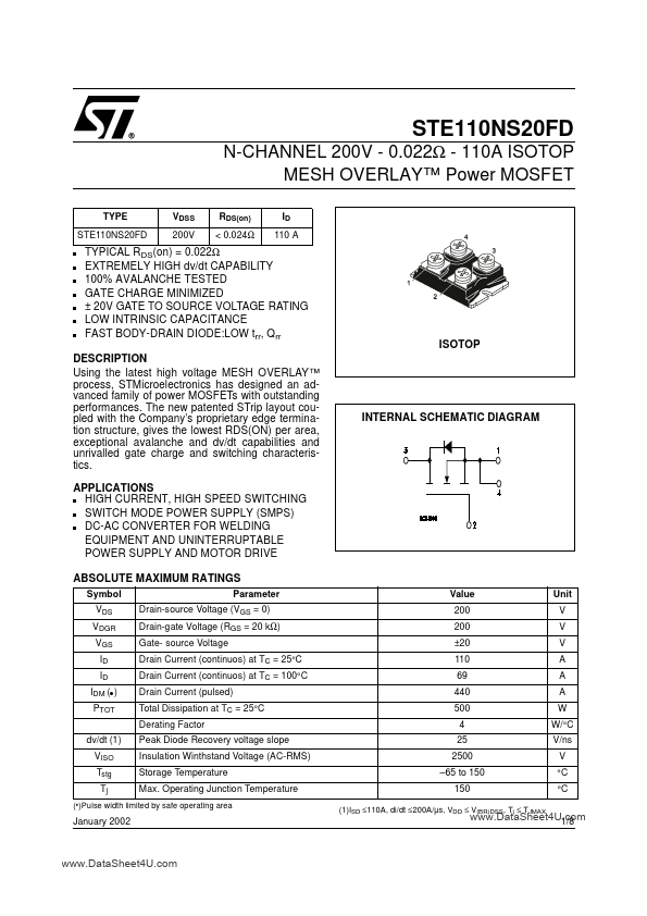
ISOTOP
DESCRIPTION Using the latest high
voltage MESH OVERLAY™ process, STMicroelectronics has designed an advanced family of power
MOSFETs with outstanding performances. The new patented STrip layout coupled with the Company’s proprietary edge termination structure, gives the lowest RDS(ON) per area, exceptional avalanche and dv/dt capabilities and unrivalled gate charge and switching characteristics. APPLICATIONS n HIGH CURRENT, HIGH SPEED SWITCHING n SWITCH MODE POWER SUPPLY (SMPS) n DC-AC CONVERTER FOR WELDING EQUIPMENT AND UNINTERRUPTABLE POWER SUPPLY AND MOTOR DRIVE ABSOLUTE MAXIMUM RATINGS
Symbol VDS VDGR VGS ID ID IDM (l) PTOT dv/dt (1) VISO Tstg Tj January 2002 Parameter Drain-source
Voltage (VGS = 0) Drain-gate
Voltage (RGS = 20 kΩ) Gate- source
Voltage Drain Current (continuos) at TC = 25°C Drain Current (continuos) at TC = 100°C Drain Current (pulsed) Total Dissipation at TC = 25°C Derating Factor Peak Diode Recovery
voltage slope Insulation Winthstand
Voltage (AC-RMS) Storage Temperature Max. Operating Junction Temperature
INTERNAL SCHEMATIC DIAGRAM
Value 200 200 ±20 110 69 440 500 4 25 2500 –65 to 150 150
(1)ISD ≤11...