www.DataSheet4U.com
S T G 8209
S amHop Microelectronics C orp. Dec,29.2005
Dual N-C hannel E nhancement Mode Field E f...
www.DataSheet4U.com
S T G 8209
S amHop Microelectronics C orp. Dec,29.2005
Dual N-C hannel E nhancement Mode Field E ffect Transistor
P R ODUC T S UMMAR Y
V DS S
20V
F E AT UR E S
( mW ) Max
ID
6A
R DS (ON)
S uper high dense cell design for low R DS (ON ).
26 @ V G S = 4.0V 40 @ V G S = 2.5V
R ugged and reliable. S urface Mount P ackage. E S D P rotected.
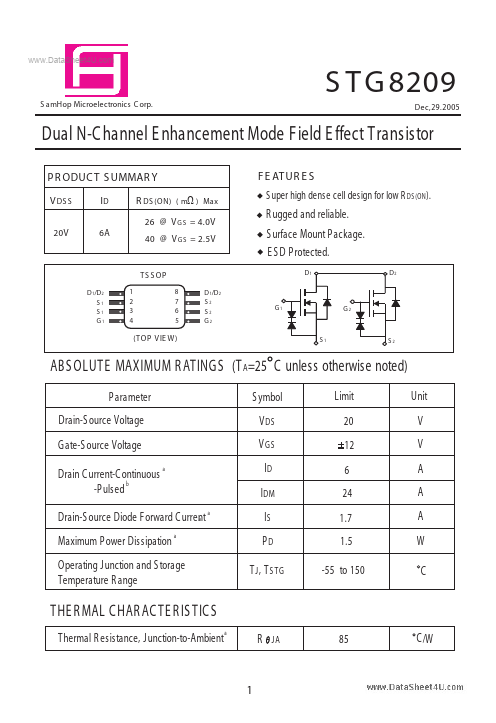
D1 D2
T S S OP
D 1/D 2 S1 S1 G1 1 2 3 4 8 7 6 5 D 1/D 2 S2 S2 G2
G1
G2
(T OP V IE W)
S1
S2
ABS OLUTE MAXIMUM R ATINGS (T A=25 C unless otherwise noted)
P arameter Drain-S ource
Voltage Gate-S ource
Voltage Drain C urrent-C ontinuous b -P ulsed
a
S ymbol V DS V GS ID IDM
a
Limit 20 12 6 24 1.7 1.5 -55 to 150
Unit V V A A A W C
Drain-S ource Diode Forward C urrent a Maximum P ower Dissipation
a
IS PD T J , T S TG
Operating Junction and S torage Temperature R ange
THE R MAL C HAR AC TE R IS TIC S
Thermal R esistance, Junction-to-Ambient
a
R JA
85
C /W
1
www.DataSheet4U.com
S T G 8209
E LE CTR ICAL CHAR ACTE R IS TICS (T A = 25 C unless otherwise noted)
Parameter OFF CHAR ACTE R IS TICS
Drain-S ource Breakdown
Voltage Zero Gate
Voltage Drain Current Gate-Body Leakage BV DS S IDS S IGS S V GS (th) R DS (ON) gFS C IS S C OS S CRSS
c
S ymbol
Condition
V GS = 0V, ID = 250uA V DS = 16V, V GS = 0V V GS = 12V,V DS = 0V V DS = V GS , ID = 250uA V GS = 4.0V, ID = 5A V GS =2.5V, ID = 3A V DS = 5V, ID =5A
Min Typ C Max Unit
20 1 10 0.5 0.8 22 30 19 693 189 136 1.5 26 40 V uA uA V
m ohm m ohm
ON CHAR ACTE R I...