STGB20NB32LZ STGB20NB32LZ-1
N-CHANNEL CLAMPED 20A - D2PAK/I2PAK INTERNALLY CLAMPED PowerMESH™ IGBT
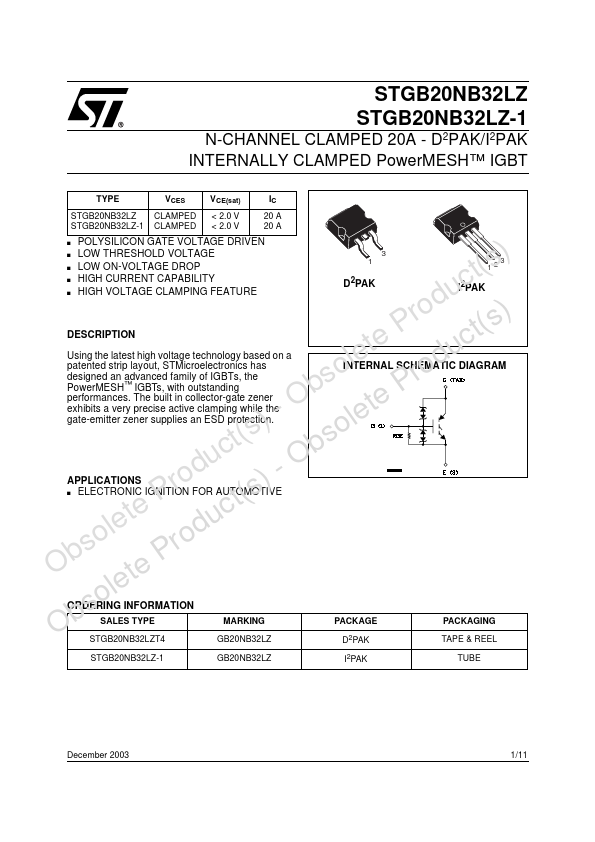
TYPE STGB20NB32LZ STG...
STGB20NB32LZ STGB20NB32LZ-1
N-CHANNEL CLAMPED 20A - D2PAK/I2PAK INTERNALLY CLAMPED PowerMESH™ IGBT
TYPE STGB20NB32LZ STGB20NB32LZ-1
s s s s s s
VCES CLAMPED CLAMPED
VCE(sat) < 2.0 V < 2.0 V
IC 20 A 20 A
3 1
3 12
POLYSILICON GATE
VOLTAGE DRIVEN LOW THRESHOLD
VOLTAGE LOW ON-
VOLTAGE DROP HIGH CURRENT CAPABILITY HIGH
VOLTAGE CLAMPING FEATURE SURFACE-MOUNTING D²PAK (TO-263) POWER PACKAGE IN TUBE (NO SUFFIX) OR IN TAPE & REEL (SUFFIX “T4”)
D 2PAK
I2PAK
DESCRIPTION Using the latest high
voltage technology based on a patented strip layout, STMicroelectronics has designed an advanced family of IGBTs, the PowerMESH™ IGBTs, with outstanding performances. The built in collector-gate zener exhibits a very precise active clamping while the gate-emitter zener supplies an ESD protection. APPLICATIONS s AUTOMOTIVE IGNITION INTERNAL SCHEMATIC DIAGRAM
ABSOLUTE MAXIMUM RATINGS
Symbol VCES VECR VGE IC IC ICM ( ) Eas Ptot ESD Tstg Tj Parameter Collector-Emitter
Voltage (VGS = 0) Reverse Battery Protection Gate-Emitter
Voltage Collector Current (continuous) at Tc = 25°C Collector Current (continuous) at Tc = 100°C Collector Current (pulsed) Single Pulse Energy Tc = 25°C Total Dissipation at Tc = 25°C Derating Factor ESD (Human Body Model) Storage Temperature Max. Operating Junction Temperature Value CLAMPED 20 CLAMPED 40 30 80 700 150 1 4 –65 to 175 175 Unit V V V A A A
mJ
W W/°C KV °C °C
()Pulse width limited by safe operating area
December 2002
1/11
STGB20NB32LZ - STGB20NB32LZ-1
THE...