STB14NM65N, STF14NM65N STI14NM65N,STP14NM65N,STW14NM65N
N-channel 650 V, 0.33 Ω, 12 A MDmesh™ II Power MOSFET TO-220, TO...
STB14NM65N, STF14NM65N STI14NM65N,STP14NM65N,STW14NM65N
N-channel 650 V, 0.33 Ω, 12 A MDmesh™ II Power
MOSFET TO-220, TO-220FP, D2PAK, I2PAK, TO-247
Features
www.DataSheet4U.com
Type
VDSS (@TJmax) 710 V 710 V 710 V 710 V 710 V
RDS(on) max < 0.38 Ω < 0.38 Ω < 0.38 Ω < 0.38 Ω < 0.38 Ω
ID
3
STI14NM65N STB14NM65N STF14NM65N STP14NM65N STW14NM65N
12 A 12 A 12 A(1) 12 A 12 A
1
2
3 12
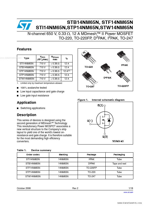
TO-220
3 1
I²PAK
D²PAK
3
1. Limited only by maximum temperature allowed ■ ■ ■
2
3
1
2
100% avalanche tested Low input capacitance and gate charge Low gate input resistance
TO-247
1
TO-220FP
Application
■
Figure 1.
Internal schematic diagram
Switching applications
Description
This series of devices is designed using the second generation of MDmesh™ Technology. This revolutionary Power
MOSFET associates a new vertical structure to the Company’s strip layout to yield one of the world’s lowest onresistance and gate charge. It is therefore suitable for the most demanding high efficiency converters. Table 1. Device summary
Marking 14NM65N 14NM65N 14NM65N 14NM65N 14NM65N Package I²PAK D²PAK TO-220FP TO-220 TO-247 Packaging Tube Tape and reel Tube Tube Tube
Order codes STI14NM65N STB14NM65N STF14NM65N STP14NM65N STW14NM65N
October 2008
Rev 2
1/18
www.st.com 18
Contents
STB/F/I/P/W14NM65N
Contents
1 2 Electrical ratings . . . . . . . . . . . . . . . . . . . . . . . . . . . . . . . . . . . . . . . . . . . . 3 Electrical characteristics . . . . . . . . . . . . . . . . . . . . . . ...