Semiconductor
STK7000
N-Channel Enhancement-Mode MOSFET
Description
• High speed switching application.
• High densit...
Semiconductor
STK7000
N-Channel Enhancement-Mode
MOSFET
Description
High speed switching application.
High density cell design for low RDS(ON).
Voltage controlled small signal switch www.DataSheet4U.com High saturation current capability.
Features
Ordering Information
Type NO. STK7000 Marking STK7000 Package Code TO-92
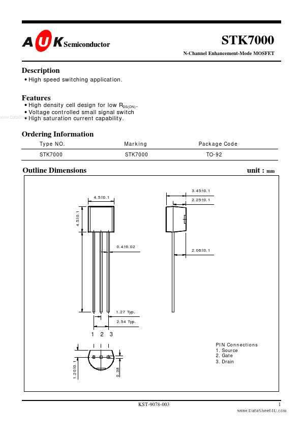
Outline Dimensions
3.45±0.1 4.5±0.1 4.5±0.1 2.25±0.1
unit : mm
0.4±0.02
2.06±0.1
1.27 Typ. 2.54 Typ.
1 2 3
PIN Connections 1. Source 2. Gate 3. Drain
0.38
1.20±0.1
KST-9078-003
1
STK7000
Absolute maximum ratings
Characteristic
Drain-Source
voltage Gate-Source
voltage Maximum Drain current Pulsed Drain Current Power dissipation Maximum Junction-to-Ambient
www.DataSheet4U.com
(Ta=25° C)
Symbol
VDSS VGS ID IDM PD RthJA T J , T stg
Ratings
60 ±20 200 500 400 312.5 -55~150
Unit
V V mA mA mW °C/W °C
Operating Junction and Storage temperature range
Electrical Characteristics
Characteristic
Drian-Source breakdown
voltage Gate-Threshold
voltage Zero Gate
voltage drain current Gate-body leakage On-state drain current * Drain-Source on-resistance * Drain-Source on-resistance * Forward transconductance * Input capacitance Output capacitance Reverse Transfer capacitance Turn-on time Turn-off time
(Ta=25° C)
Symbol
BVDSS VGS(t h) IDSS IGSS ID(on) RDS(ON) RDS(ON) g fs C iss C oss C rss tON tOFF
Test Condition
ID =10µA, VGS =0 ID =1mA, V DS =VGS VDS =48V, V GS =0 VDS =0V, VGS =± 15V VDS =10V, V GS =4.5V VGS =4.5V, ID =0.075A VGS =10V, I D =0.5A ...