G P
STM102D
Ver 1.0
S a mHop Microelectronics C orp.
Dual Enhancement Mode Field Effect Transistor (N and P Channel)
...
G P
STM102D
Ver 1.0
S a mHop Microelectronics C orp.
Dual Enhancement Mode Field Effect Transistor (N and P Channel)
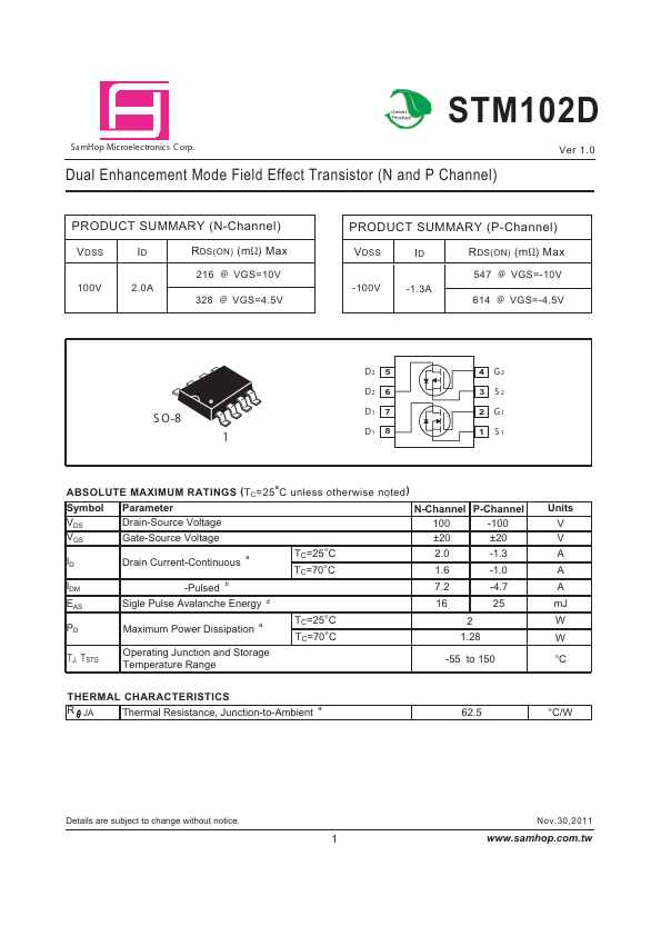
PRODUCT SUMMARY (N-Channel)
V DSS
100V
PRODUCT SUMMARY (P-Channel)
V DSS
-100V
ID
2.0A
R DS(ON) (m Ω) Max
216 @ VGS=10V
ID
-1.3A
R DS(ON) (m Ω) Max
547 @ VGS=-10V 614 @ VGS=-4.5V
328 @ VGS=4.5V
D2 D2
5 6 7 8
4 3 2 1
G2 S2 G1 S1
S O-8 1
D1 D1
ABSOLUTE MAXIMUM RATINGS ( T C=25 °C unless otherwise noted ) Symbol VDS VGS ID IDM EAS PD TJ, TSTG Parameter Drain-Source
Voltage Gate-Source
Voltage Drain Current-Continuous -Pulsed
b d a
TC=25°C TC=70°C
N-Channel P-Channel -100 100 ±20 ±20 -1.3 2.0 1.6 7.2 16 -1.0 -4.7 25 2 1.28 -55 to 150
Units V V A A A mJ W W °C
Sigle Pulse Avalanche Energy Maximum Power Dissipation
a
TC=25°C TC=70°C
Operating Junction and Storage Temperature Range
THERMAL CHARACTERISTICS R JA Thermal Resistance, Junction-to-Ambient
a
62.5
°C/W
Details are subject to change without notice.
Nov,30,2011
1
www.samhop.com.tw
STM102D
Ver 1.0
N-Channel ELECTRICAL CHARACTERISTICS ( T C=25 °C unless otherwise noted )
4 Symbol
Parameter
Conditions
VGS=0V , ID=250uA VDS=80V , VGS=0V
Min 100
Typ
Max
Units V uA nA
OFF CHARACTERISTICS Drain-Source Breakdown
Voltage BVDSS Zero Gate
Voltage Drain Current IDSS Gate-Body Leakage Current IGSS ON CHARACTERISTICS Gate Threshold
Voltage VGS(th) RDS(ON) gFS Drain-Source On-State Resistance Forward Transconductance
c
VGS= ±20V , VDS=0V
1 ±100
VDS=VGS , ID=250uA VGS=10V , ID=1.0A VG...