www.DataSheet4U.com
STP130NS04ZB STB130NS04ZB - STW130NS04ZB
N-CHANNEL CLAMPED - 7 mΩ - 80A TO-220/D²PAK/TO-247 FULLY P...
www.DataSheet4U.com
STP130NS04ZB STB130NS04ZB - STW130NS04ZB
N-CHANNEL CLAMPED - 7 mΩ - 80A TO-220/D²PAK/TO-247 FULLY PROTECTED MESH OVERLAY™
MOSFET
Table 1: General Features
TYPE STP130NS04ZB STB130NS04ZB STW130NS04ZB
s s s s
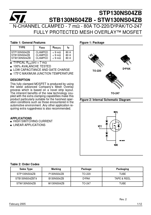
Figure 1: Package
RDS(on) < 9 mΩ < 9 mΩ < 9 mΩ ID 80 A 80 A 80 A
3
3 1 2
VDSS CLAMPED CLAMPED CLAMPED
TYPICAL RDS(on) = 7 mΩ 100% AVALANCHE TESTED LOW CAPACITANCE AND GATE CHARGE 175°C MAXIMUM JUNCTION TEMPERATURE
1
TO-220
D²PAK
DESCRIPTION This fully clamped
MOSFET is produced by using the latest advanced Company’s Mesh Overlay process which is based on a novel strip layout. The inherent benefits of the new technology coupled with the extra clamping capabilities make this product particularly suitable for the harshest operation conditions such as those encountered in the automotive environment .Any other application requiring extra ruggedness is also recommended.
3 2 1
TO-247
Figure 2: Internal Schematic Diagram
APPLICATIONS s HIGH SWITCHING CURRENT s LINEAR APPLICATIONS
Table 2: Order Codes
Sales Type STP130NS04ZB STB130NS04ZBT4 STW130NS04ZB Marking P130NS04ZB B130NS04ZB W130NS04ZB Package TO-220 D²PAK TO-247 Packaging TUBE TAPE & REEL TUBE
Rev. 2 February 2005 1/12
STP130NS04ZB - STB130NS04ZB - STW130NS04ZB
Table 3: Absolute Maximum ratings
Symbol VDS VDG VGS ID ID IDG IGS IDM ( ) PTOT VESD(G-S) Tj Tstg Parameter Drain-source
Voltage (VGS = 0) Drain-gate
Voltage Gate- source
Voltage Drain Current (continuous) at TC = 25°C Drain Current...