STP16NK65Z STB16NK65Z-S
N-CHANNEL 650V - 0.38Ω - 13A TO-220 / I2SPAK Zener - Protected SuperMESH™ MOSFET
Table 1: Genera...
STP16NK65Z STB16NK65Z-S
N-CHANNEL 650V - 0.38Ω - 13A TO-220 / I2SPAK Zener - Protected SuperMESH™
MOSFET
Table 1: General Features
TYPE STP16NK65Z STB16NK65Z-S
s s s s s s
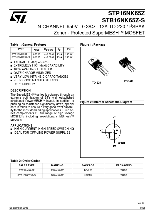
Figure 1: Package
ID 13 A 13 A Pw 190 W 190 W
VDSS 650 V 650 V
RDS(on) < 0.50 Ω < 0.50 Ω
TYPICAL RDS(on) = 0.38Ω EXTREMELY HIGH dv/dt CAPABILITY 100% AVALANCHE TESTED GATE CHARGE MINIMIZED VERY LOW INTRINSIC CAPACITANCES VERY GOOD MANUFACTURING REPEATIBILITY
3 12
3 1 2
TO-220
I²SPAK
DESCRIPTION The SuperMESH™ series is obtained through an extreme optimization of ST’s well established stripbased PowerMESH™ layout. In addition to pushing on-resistance significantly down, special care is taken to ensure a very good dv/dt capability for the most demanding applications. Such series complements ST full range of high
voltage MOSFETs including revolutionary MDmesh™ products. APPLICATIONS s HIGH CURRENT, HIGH SPEED SWITCHING s IDEAL FOR OFF-LINE POWER SUPPLIES
Figure 2: Internal Schematic Diagram
Table 2: Order Codes
SALES TYPE STP16NK65Z STB16NK65Z-S MARKING P16NK65Z B16NK65Z PACKAGE TO-220 I²SPAK PACKAGING TUBE TUBE
Rev. 3 September 2005 1/12
STP16NK65Z - STB16NK65Z-S
Table 3: Absolute Maximum ratings
Symbol VDS VDGR VGS ID ID IDM (*) PTOT VESD(G-S) dv/dt (1) Tj Tstg Parameter Drain-source
Voltage (VGS = 0) Drain-gate
Voltage (RGS = 20 kΩ) Gate- source
Voltage Drain Current (continuous) at TC = 25°C Drain Current (continuous) at TC = 100°C Drain Current (pulsed) Total Dissipation at TC = 25°C Derating ...