N-CHANNEL 30V - 0.008Ω - 70A TO-220/I2PAK LOW GATE CHARGE STripFET™ POWER MOSFET
TYPE STP70NF03L STB70NF03L-1
s s s s s
...
N-CHANNEL 30V - 0.008Ω - 70A TO-220/I2PAK LOW GATE CHARGE STripFET™ POWER
MOSFET
TYPE STP70NF03L STB70NF03L-1
s s s s s
STP70NF03L STB70NF03L-1
VDSS 30 V 30 V
RDS(on) < 0.01 Ω < 0.01 Ω
ID 70 A 70 A
TYPICAL RDS(on) = 0.008 Ω TYPICAL Qg = 35 nC @ 10 V OPTIMAL RDS(on) x Qg TRADE-OFF CONDUCTION LOSSES REDUCED SWITCHING LOSSES REDUCED TO-220
3 1 2
3 12
I2PAK
DESCRIPTION This application specific Power
Mosfet is the third generation of STMicroelectronics unique “Single Feature Size ™” strip-based process. The resulting transistor shows the best trade-off between onresistance and gate charge. When used as high and low side in buck regulators, it gives the best performance in terms of both conduction and switching losses. This is extremely important for motherboards where fast switching and high efficiency are of paramount importance. APPLICATIONS s SPECIFICALLY DESIGNED AND OPTIMISED FOR HIGH EFFICIENCY CPU CORE DC/DC CONVERTERS
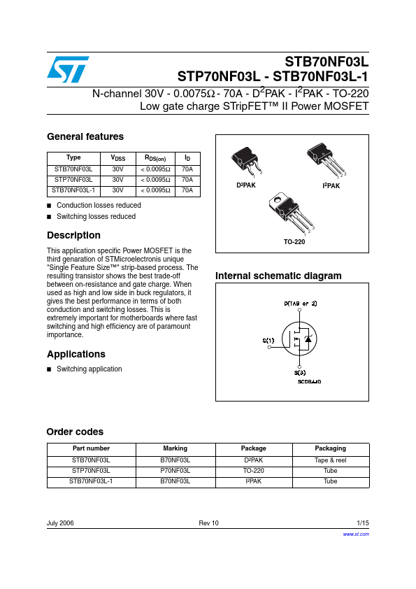
INTERNAL SCHEMATIC DIAGRAM
ABSOLUTE MAXIMUM RATINGS
Symbol VDS VDGR VGS ID ID IDM (q) PTOT dv/dt (1) Tstg Tj Parameter Drain-source
Voltage (VGS = 0) Drain-gate
Voltage (RGS = 20 kΩ) Gate- source
Voltage Drain Current (continuos) at TC = 25°C Drain Current (continuos) at TC = 100°C Drain Current (pulsed) Total Dissipation at TC = 25°C Derating Factor Peak Diode Recovery
voltage slope Storage Temperature Max. Operating Junction Temperature Value 30 30 ± 15 70 50 280 100 0.67 4 –65 to 175 175
(1) ISD ≤70A, di/dt ≤290A/µs, VDD =24 V ; Tj ≤ TJMAX.
Uni...