S T S 2622
S amHop Microelectronics C orp. F eb,25 2005 V er1.1
Dual N-C hannel E nhancement Mode Field E ffect Transis...
S T S 2622
S amHop Microelectronics C orp. F eb,25 2005 V er1.1
Dual N-C hannel E nhancement Mode Field E ffect Transistor
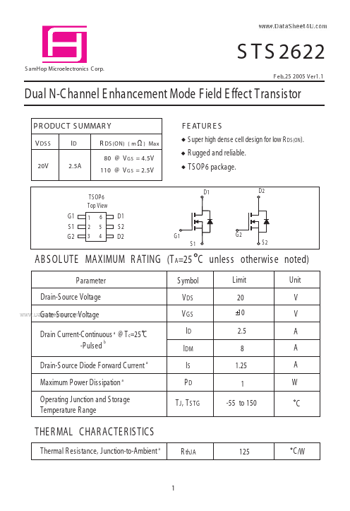
P R ODUC T S UMMAR Y
V DS S
20V
F E AT UR E S
( m W ) Max
ID
2.5A
R DS (ON)
S uper high dense cell design for low R DS (ON ).
80 @ V G S = 4.5V 110 @ V G S = 2.5V
R ugged and reliable. TS OP 6 package.
D1 D2
TS OP 6 Top View
G1 S1 G2
1 2 3
6 5 4
D1 S2 D2
G1 S1
G2 S2
AB S OL UTE MAXIMUM R ATING (T A =25 C unles s otherwis e noted)
P arameter Drain-S ource
Voltage
www.DataSheet4U.com Gate-S ource
Voltage
S ymbol V DS V GS ID IDM IS PD T J , T S TG
Limit 20 10 2.5 8 1.25 1 -55 to 150
Unit V V A A A W C
Drain C urrent-C ontinuous a @ T c=25 C b -P ulsed Drain-S ource Diode Forward C urrent a Maximum P ower Dissipation a Operating Junction and S torage Temperature R ange
THE R MAL CHAR ACTE R IS TICS
Thermal R esistance, Junction-to-Ambient a R thJA 125 C /W
1
S T S 2622
E LE CTR ICAL CHAR ACTE R IS TICS (T A =25 C unless otherwise noted)
Parameter OFF CHAR ACTE R IS TICS
Drain-S ource Breakdown
Voltage Zero Gate
Voltage Drain Current Gate-Body Leakage BV DS S IDS S IGS S V GS (th) R DS (ON) ID(ON) gFS C IS S C OS S CRSS
c
S ymbol
Condition
V GS = 0V, ID = 250uA V DS = 16V, V GS = 0V V GS = 10V, V DS = 0V V DS = V GS , ID = 250uA V GS = 4.5V, ID =2A V GS = 2.5V, ID= 1A V DS = 5V, V GS = 4.5V V DS = 5V, ID =2.5A
Min Typ C Max Unit
20 1 100 0.5 0.8 65 90 6 7 220 67 50 1.5 80 110 V uA nA V
m-ohm m-ohm
ON CHAR ACTE R IS TICS b
Gate Thresh...