STU6NA90
N - CHANNEL ENHANCEMENT MODE FAST POWER MOS TRANSISTOR
PRELIMINARY DATA TYPE STU6NA90
www.DataSheet4U.com s TYP...
STU6NA90
N - CHANNEL ENHANCEMENT MODE FAST POWER MOS TRANSISTOR
PRELIMINARY DATA TYPE STU6NA90
www.DataSheet4U.com s TYPICAL
s s s s s s
V DSS 900 V
R DS(on) <2Ω
ID 5.8 A
RDS(on) = 1.5 Ω ± 30V GATE TO SOURCE
VOLTAGE RATING REPETITIVE AVALANCHE TESTED LOW INTRINSIC CAPACITANCE 100% AVALANCHE TESTED GATE CHARGE MINIMIZED REDUCED THRESHOLD
VOLTAGE SPREAD
1
2
3
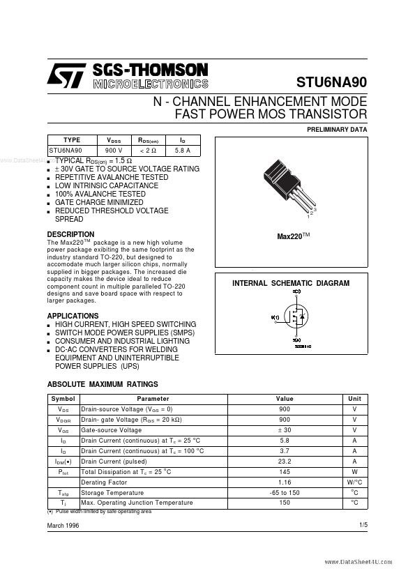
The Max220 TM package is a new high volume power package exibiting the same footprint as the industry standard TO-220, but designed to accomodate much larger silicon chips, normally supplied in bigger packages. The increased die capacity makes the device ideal to reduce component count in multiple paralleled TO-220 designs and save board space with respect to larger packages.
DESCRIPTION
Max220TM
INTERNAL SCHEMATIC DIAGRAM
APPLICATIONS s HIGH CURRENT, HIGH SPEED SWITCHING s SWITCH MODE POWER SUPPLIES (SMPS) s CONSUMER AND INDUSTRIAL LIGHTING s DC-AC CONVERTERS FOR WELDING EQUIPMENT AND UNINTERRUPTIBLE POWER SUPPLIES (UPS) ABSOLUTE MAXIMUM RATINGS
Symbol V DS VDGR V GS ID ID I DM ( ) P tot T stg Tj Parameter Drain-source
Voltage (V GS = 0) Drain- gate
Voltage (R GS = 20 k Ω ) Gate-source
Voltage Drain Current (continuous) at T c = 25 o C Drain Current (continuous) at T c = 100 o C Drain Current (pulsed) Total Dissipation at T c = 25 C Derating Factor Storage Temperature Max. Operating Junction Temperature
o
Value 900 900 ± 30 5.8 3.7 23.2 145 1.16 -65 to 150 150
Unit V V V A A A W W/ o C
o o
C C
() Pulse ...