N-CHANNEL 900V - 1.1 Ω - 7.3 A Max220/Max220I PowerMesh™ MOSFET
TYPE STU7NB90 STU7NB90I www.DataSheet4U.com
s s s s s s
...
N-CHANNEL 900V - 1.1 Ω - 7.3 A Max220/Max220I PowerMesh™
MOSFET
TYPE STU7NB90 STU7NB90I www.DataSheet4U.com
s s s s s s
STU7NB90 STU7NB90I
VDSS 900 V 900 V
RDS(on) < 1.45 Ω < 1.45 Ω
ID 7.3 A 7.3 A
TYPICAL RDS(on) = 1.1 Ω EXTREMELY HIGH dv/dt CAPABILITY 100% AVALANCHE TESTED VERY LOW INTRINSIC CAPACITANCES GATE CHARGE MINIMIZED REDUCED
VOLTAGE SPREAD
1
2
3
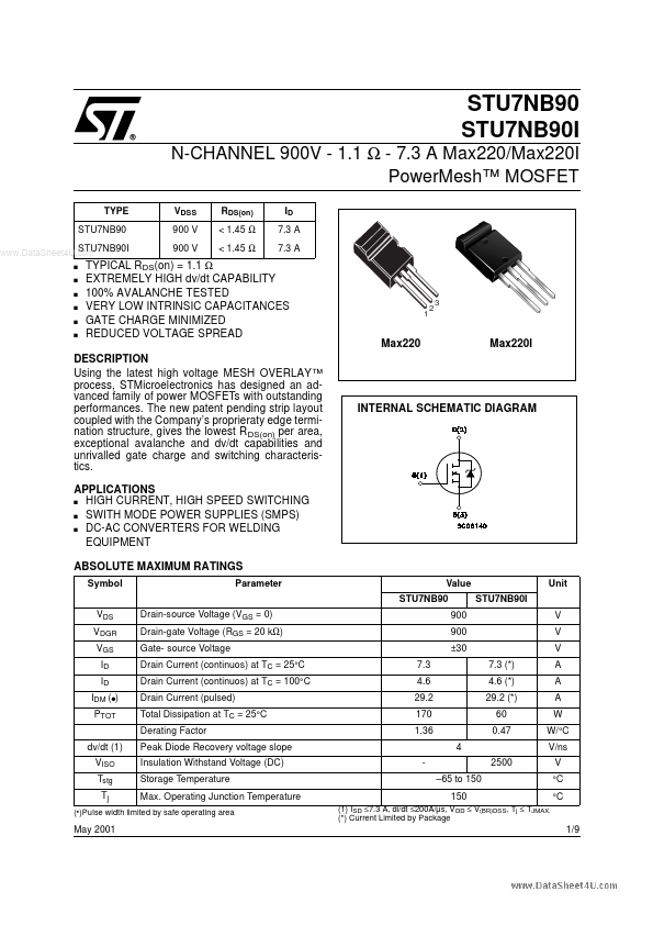
Max220
Max220I
DESCRIPTION Using the latest high
voltage MESH OVERLAY ™ process, STMicroelectronics has designed an advanced family of power
MOSFETs with outstanding performances. The new patent pending strip layout coupled with the Company’s proprieraty edge termination structure, gives the lowest R DS(on) per area, exceptional avalanche and dv/dt capabilities and unrivalled gate charge and switching characteristics. APPLICATIONS s HIGH CURRENT, HIGH SPEED SWITCHING s SWITH MODE POWER SUPPLIES (SMPS) s DC-AC CONVERTERS FOR WELDING EQUIPMENT ABSOLUTE MAXIMUM RATINGS
Symbol VDS VDGR VGS ID ID IDM (q) PTOT dv/dt (1) VISO Tstg Tj Parameter Drain-source
Voltage (VGS = 0) Drain-gate
Voltage (RGS = 20 kΩ) Gate- source
Voltage Drain Current (continuos) at TC = 25°C Drain Current (continuos) at TC = 100°C Drain Current (pulsed) Total Dissipation at TC = 25°C Derating Factor Peak Diode Recovery
voltage slope Insulation Withstand
Voltage (DC) Storage Temperature Max. Operating Junction Temperature
INTERNAL SCHEMATIC DIAGRAM
Value STU7NB90 900 900 ±30 7.3 4.6 29.2 170 1.36 4 –65 to 150 150 2500 7.3 (*) 4.6 (*) 29.2 (*) 60 ...