SW20N50D
Features
Low gate charge 100% avalanche tested Improved dv/dt capability RoHS compliant JEDEC Qualifi...
SW20N50D
Features
Low gate charge 100% avalanche tested Improved dv/dt capability RoHS compliant JEDEC Qualification
N-channel
MOSFET BVDSS 500V ID 20A RDS(on) < 0.3W
Device SW20N50D
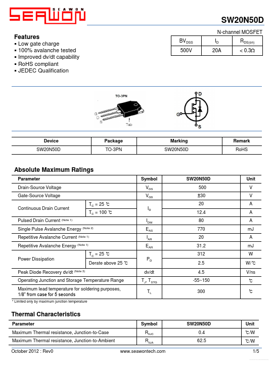
Package TO-3PN
Marking SW20N50D
Remark RoHS
Absolute Maximum Ratings
Parameter Drain-Source
Voltage Gate-Source
Voltage Continuous Drain Current Pulsed Drain Current (Note 1) Single Pulse Avalanche Energy (Note 2) Repetitive Avalanche Current (Note 1) Repetitive Avalanche Energy (Note 1) Power Dissipation Peak Diode Recovery dv/dt (Note 3) Operating Junction and Storage Temperature Range Maximum lead temperature for soldering purposes, 1/8” from case for 5 seconds
* Limited only by maximum junction temperature
Symbol VDS VGS TC = 25 ℃ TC = 100 ℃ ID IDM EAS IAR EAR TC = 25 ℃ Derate above 25 ℃ PD dv/dt TJ, TSTG TL
SW20N50D 500 ±30 20 12.4 80 770 20 31.2 312 2.5 4.5 -55~150 300
Unit V V A A A mJ A mJ W W/℃ V/ns ℃ ℃
Thermal Characteristics
Parameter Maximum Thermal resistance, Junction-to-Case Maximum Thermal resistance, Junction-to-Ambient October 2012 : Rev0 Symbol RqJC RqJA www.seawontech.com SW20N50D 0.4 62.5 Unit ℃/W ℃/W 1/5
Free Datasheet http://www.datasheet4u.com/
SW20N50D
Electrical Characteristics : TC=25℃, unless otherwise noted
Parameter Symbol Test condition Min Typ Max Units
OFF
Drain-Source Breakdown
Voltage Zero Gate
Voltage Drain Current Forward Gate-Source Leakage Current Reverse Gate-Source Leakage Current BVDSS IDSS IGSSF IGSSR VGS = 0 V, ID = 250 µA VDS = 500...