6-BIT 2:1 MUX-REGISTER
SEMICONDUCTOR
SYNERGY
6-BIT 2:1 MUX-REGISTER
SY10E167 SY100E167
SY10E167 SY100E167
FEATURES
s s s s s s s s s s s 1...
Description
SEMICONDUCTOR
SYNERGY
6-BIT 2:1 MUX-REGISTER
SY10E167 SY100E167
SY10E167 SY100E167
FEATURES
s s s s s s s s s s s 1000MHz min. operating frequency Extended 100E VEE range of –4.2V to –5.5V 800ps max. clock to output Single-ended outputs Asynchronous Master Reset Dual clocks Fully compatible with industry standard 10KH, 100K ECL levels Internal 75KΩ input pulldown resistors ESD protection of 2000V Fully compatible with Motorola MC10E/100E167 Available in 28-pin PLCC package
DESCRIPTION
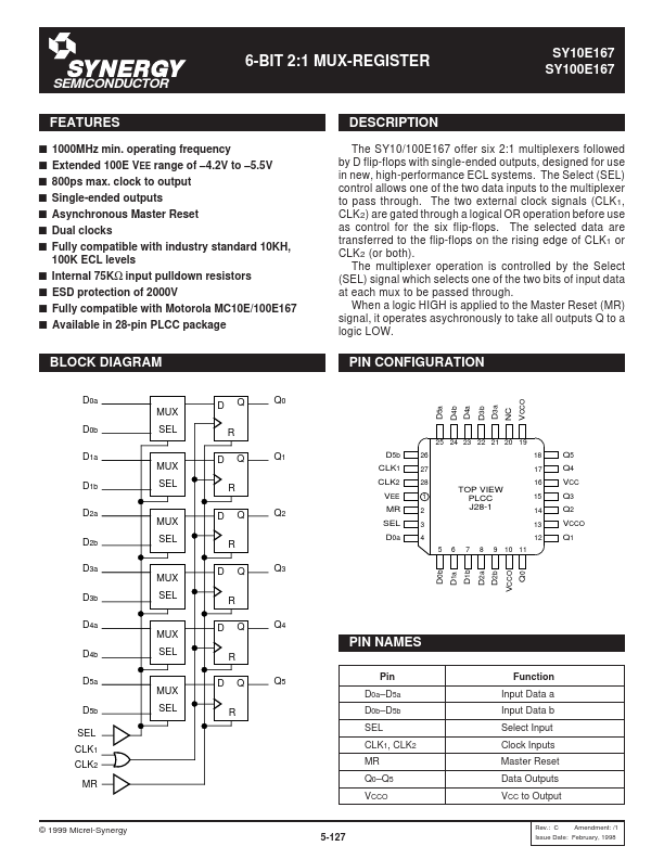
The SY10/100E167 offer six 2:1 multiplexers followed by D flip-flops with single-ended outputs, designed for use in new, high-performance ECL systems. The Select (SEL) control allows one of the two data inputs to the multiplexer to pass through. The two external clock signals (CLK1, CLK2) are gated through a logical OR operation before use as control for the six flip-flops. The selected data are transferred to the flip-flops on the rising edge of CLK1 or CLK2 (or both). The multiplexer operation is controlled by the Select (SEL) signal which selects one of the two bits of input data at each mux to be passed through. When a logic HIGH is applied to the Master Reset (MR) signal, it operates asychronously to take all outputs Q to a logic LOW.
BLOCK DIAGRAM
D0a MUX D0b D1a MUX D1b D2a MUX D2b D3a MUX D3b D4a MUX D4b D5a MUX D5b SEL CLK1 CLK2 MR SEL SEL D R SEL D R Q Q5 SEL D R Q Q4 SEL D R Q Q3 SEL D R Q Q2 D R Q Q0
PIN CONFIGURATION
D3b D3a NC VCCO
D5a D5b CLK1 CLK2 VEE MR SEL D0a
25 24 2...
Similar Datasheet