Si4542DY
Si4542DY
30V Complementary PowerTrench MOSFET
General Description
Features
This complementary MOSFET devi...
Si4542DY
Si4542DY
30V Complementary PowerTrench
MOSFET
General Description
Features
This complementary
MOSFET device is produced using ON Semiconductor’s advanced PowerTrench process that has been especially tailored to minimize the on-state resistance and yet maintain low gate charge for superior switching performance.
Applications
DC/DC converter
Q1: N-Channel
6 A, 30 V
RDS(on) = 28 mΩ @ VGS = 10V RDS(on) = 35 mΩ @ VGS = 4.5V
Q2: P-Channel
–6 A, –30 V
RDS(on) = 32 mΩ @ VGS = –10V RDS(on) = 45 mΩ @ VGS = –4.5V
Power management
DD2 DD2 DD1 DD1
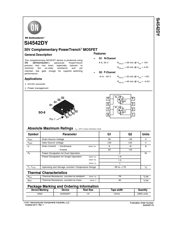
SO-8
Pin 1 SO-8
G2
S2 G
G1
S1 S
S
S
Q2
5
6
Q1
7
8
4 3 2 1
Absolute Maximum Ratings TA = 25°C unless otherwise noted
Symbol
Parameter
VDSS VGSS ID PD
TJ, TSTG
Drain-Source
Voltage
Gate-Source
Voltage
Drain Current - Continuous - Pulsed
Power Dissipation for Dual Operation Power Dissipation for Single Operation
(Note 1a)
(Note 1a) (Note 1b)
(Note 1c)
Operating and Storage Junction Temperature Range
Thermal Characteristics
RθJA Thermal Resistance, Junction-to-Ambient
RθJC Thermal Resistance, Junction-to-Case
(Note 1a) (Note 1)
Package Marking and Ordering Information
Device Marking
Device
Reel Size
4542
Si4542DY
13”
Q1 Q2
30 –30 ±20 ±20
6 –6 20 –20
2 1.6 1.2 1 –55 to +175
78 40
Units
V V A W
°C
°C/W °C/W
Tape width 12mm
Quantity 2500 units
2001 Semiconductor Components Industries, LLC. October-2017, Rev 1
Publication Order Number: Si4542DY/D
Si4542DY
Electrical Characteristics
Sym...