N-Channel 40-V (D-S) MOSFET
Si7156DP
Vishay Siliconix
PRODUCT SUMMARY
VDS (V) 40
RDS(on) (Ω) 0.0035 at VGS = 10 V 0....
N-Channel 40-V (D-S)
MOSFET
Si7156DP
Vishay Siliconix
PRODUCT SUMMARY
VDS (V) 40
RDS(on) (Ω) 0.0035 at VGS = 10 V 0.0047 at VGS = 4.5 V
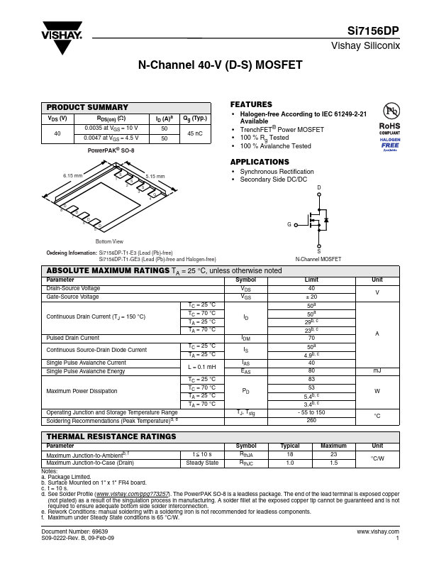
PowerPAK® SO-8
ID (A)a 50 50
Qg (Typ.) 45 nC
6.15 mm
D 8D
7 D
6 D
5
S 1S
5.15 mm
2 S
3G
4
FEATURES Halogen-free According to IEC 61249-2-21
Available TrenchFET® Power
MOSFET 100 % Rg Tested 100 % Avalanche Tested
APPLICATIONS Synchronous Rectification Secondary Side DC/DC
D
G
Bottom View
Ordering Information: Si7156DP-T1-E3 (Lead (Pb)-free) Si7156DP-T1-GE3 (Lead (Pb)-free and Halogen-free)
ABSOLUTE MAXIMUM RATINGS TA = 25 °C, unless otherwise noted
Parameter
Symbol
Drain-Source
Voltage Gate-Source
Voltage
VDS VGS
Continuous Drain Current (TJ = 150 °C) Pulsed Drain Current
TC = 25 °C TC = 70 °C TA = 25 °C TA = 70 °C
ID IDM
Continuous Source-Drain Diode Current
Single Pulse Avalanche Current Single Pulse Avalanche Energy
TC = 25 °C TA = 25 °C
L = 0.1 mH
IS
IAS EAS
Maximum Power Dissipation
Operating Junction and Storage Temperature Range Soldering Recommendations (Peak Temperature)d, e
TC = 25 °C TC = 70 °C TA = 25 °C TA = 70 °C
PD TJ, Tstg
S N-Channel
MOSFET
Limit 40 ± 20 50a 50a
29b, c 23b, c
70 50a 4.9b, c 40 80 83 53 5.4b, c 3.4b, c - 55 to 150 260
Unit V
A
mJ W °C
THERMAL RESISTANCE RATINGS
Parameter
Symbol
Typical
Maximum
Unit
Maximum Junction-to-Ambientb, f Maximum Junction-to-Case (Drain)
t ≤ 10 s Steady State
RthJA RthJC
18 1.0
23 °C/W
1.5
Notes: a. Package Limited. b. Surface Mou...