P-Channel 150 V (D-S) MOSFET
Si7317DN
Vishay Siliconix
PRODUCT SUMMARY
VDS (V) - 150
RDS(on) () Max. 1.2 at VGS = -...
P-Channel 150 V (D-S)
MOSFET
Si7317DN
Vishay Siliconix
PRODUCT SUMMARY
VDS (V) - 150
RDS(on) () Max. 1.2 at VGS = - 10 V 1.3 at VGS = - 6 V
ID (A)f - 2.8 - 2.7
Qg (Typ.) 6.5 nC
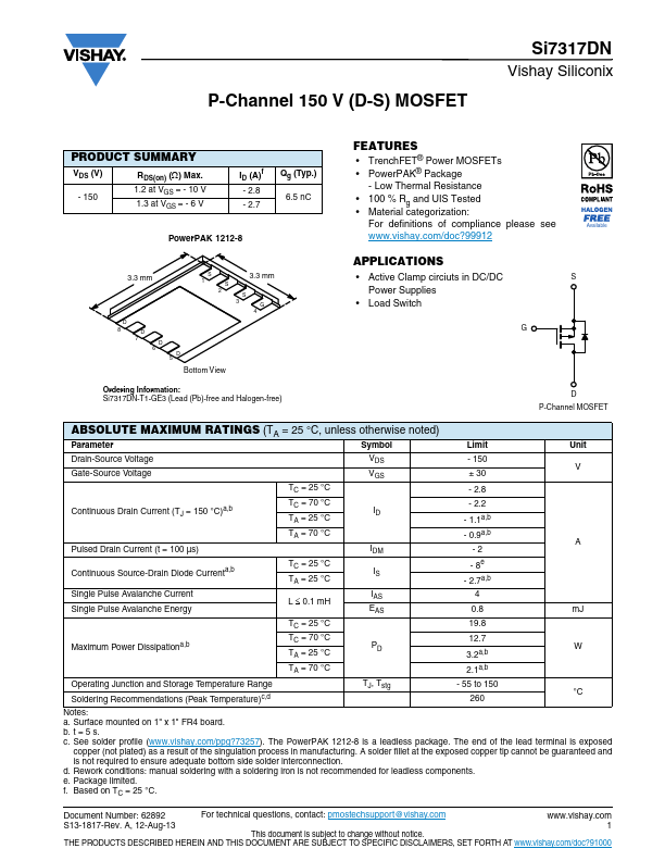
PowerPAK 1212-8
FEATURES TrenchFET® Power
MOSFETs PowerPAK® Package
- Low Thermal Resistance
100 % Rg and UIS Tested Material categorization:
For definitions of compliance please see www.vishay.com/doc?99912
Available
3.3 mm
S 1S
3.3 mm
2 S
3G
4
D
8D 7 D 6 D 5
Bottom View
Ordering Information: Si7317DN-T1-GE3 (Lead (Pb)-free and Halogen-free)
APPLICATIONS Active Clamp circiuts in DC/DC
Power Supplies Load Switch
G
S
D P-Channel
MOSFET
ABSOLUTE MAXIMUM RATINGS (TA = 25 °C, unless otherwise noted)
Parameter
Symbol
Limit
Unit
Drain-Source
Voltage Gate-Source
Voltage
VDS - 150
VGS
± 30
V
TC = 25 °C
- 2.8
Continuous Drain Current (TJ = 150 °C)a,b
TC = 70 °C TA = 25 °C
ID
- 2.2 - 1.1a,b
Pulsed Drain Current (t = 100 µs)
TA = 70 °C
IDM
- 0.9a,b -2
A
Continuous Source-Drain Diode Currenta,b
TC = 25 °C TA = 25 °C
IS
- 8e - 2.7a,b
Single Pulse Avalanche Current Single Pulse Avalanche Energy
L 0.1 mH
IAS EAS
4 0.8
mJ
TC = 25 °C
19.8
Maximum Power Dissipationa,b
TC = 70 °C TA = 25 °C
PD
12.7 3.2a,b
W
TA = 70 °C
2.1a,b
Operating Junction and Storage Temperature Range Soldering Recommendations (Peak Temperature)c,d
TJ, Tstg
- 55 to 150 260
°C
Notes: a. Surface mounted on 1" x 1" FR4 board. b. t = 5 s. c. See solder profile (www.vishay.co...