Si7366DP
Vishay Siliconix
N-Channel 20-V (D-S) MOSFET
PRODUCT SUMMARY
VDS (V) 20 RDS(on) (Ω) 0.0055 at VGS = 10 V 0.00...
Si7366DP
Vishay Siliconix
N-Channel 20-V (D-S)
MOSFET
PRODUCT SUMMARY
VDS (V) 20 RDS(on) (Ω) 0.0055 at VGS = 10 V 0.009 at VGS = 4.5 V ID (A) 20 16
FEATURES
Halogen-free available
TrenchFET® Power
MOSFET
Qg Optimized
RoHS
COMPLIANT
APPLICATIONS
Synchronous Rectifier for DC/DC
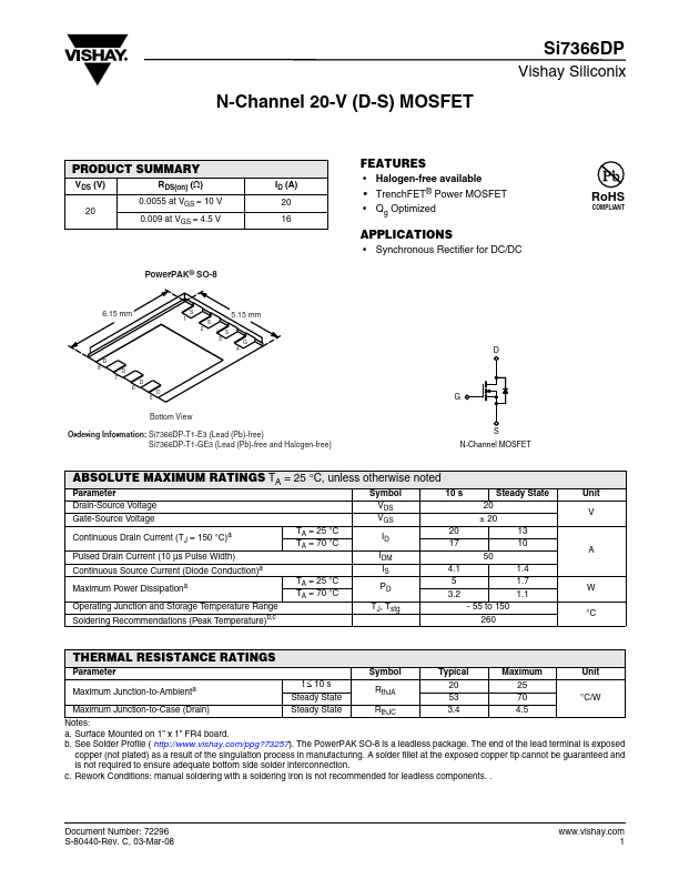
PowerPAK® SO-8
6.15 mm
S 1 2 3 S S
5.15 mm
G 4
D
D 8 7 6 5 D D D
G
Bottom View Ordering Information: Si7366DP-T1-E3 (Lead (Pb)-free) Si7366DP-T1-GE3 (Lead (Pb)-free and Halogen-free) S N-Channel
MOSFET
ABSOLUTE MAXIMUM RATINGS TA = 25 °C, unless otherwise noted
Parameter Drain-Source
Voltage Gate-Source
Voltage Continuous Drain Current (TJ = 150 °C)a Pulsed Drain Current (10 µs Pulse Width) Continuous Source Current (Diode Conduction)a Maximum Power Dissipationa Operating Junction and Storage Temperature Range Soldering Recommendations (Peak Temperature)b,c TA = 25 °C TA = 70 °C TA = 25 °C TA = 70 °C Symbol VDS VGS ID IDM IS PD TJ, Tstg 10 s Steady State 20 ± 20 13 10 50 1.4 1.7 1.1 - 55 to 150 260 Unit V
20 17 4.1 5 3.2
A
W °C
THERMAL RESISTANCE RATINGS
Parameter Maximum Junction-to-Ambient
a
Symbol t ≤ 10 s Steady State Steady State RthJA
°C/W RthJC Maximum Junction-to-Case (Drain) Notes: a. Surface Mounted on 1” x 1” FR4 board. b. See Solder Profile ( http://www.vishay.com/ppg?73257). The PowerPAK SO-8 is a leadless package. The end of the lead terminal is exposed copper (not plated) as a result of the singulation process in manufacturing. A solder fillet at the exposed co...