NTD60N02R Power MOSFET
Features
62 A, 24 V, N−Channel, DPAK
• • • • • •
Planar HD3e Process for Fast Switching Performa...
NTD60N02R Power
MOSFET
Features
62 A, 24 V, N−Channel, DPAK
Planar HD3e Process for Fast Switching Performance Low RDS(on) to Minimize Conduction Loss Low Ciss to Minimize Driver Loss Low Gate Charge Optimized for High Side Switching Requirements in High−Efficiency DC−DC Converters Pb−Free Packages are Available
http://onsemi.com
V(BR)DSS 24 V
RDS(on) TYP 8.4 mW @ 10 V
ID MAX 62 A
MAXIMUM RATINGS (TJ = 25°C unless otherwise noted)
Rating Drain−to−Source
Voltage Gate−to−Source
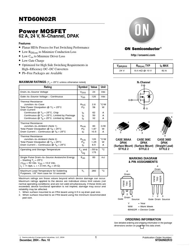
Voltage − Continuous Thermal Resistance Junction−to−Case Total Power Dissipation @ TC = 25°C Drain Current Continuous @ TC = 25°C, Chip Continuous @ TC = 25°C, Limited by Package Continuous @ TA = 25°C, Limited by Wires Thermal Resistance Junction−to−Ambient (Note 1) Total Power Dissipation @ TA = 25°C Drain Current − Continuous @ TA = 25°C Thermal Resistance Junction−to−Ambient (Note 2) Total Power Dissipation @ TA = 25°C Drain Current − Continuous @ TA = 25°C Operating and Storage Temperature Single Pulse Drain−to−Source Avalanche Energy − Starting TJ = 25°C (VDD = 50 Vdc, VGS = 10.0 Vdc, IL = 11 Apk, L = 1.0 mH, RG = 25 W) Maximum Lead Temperature for Soldering Purposes, 1/8″ from case for 10 seconds Symbol VDSS VGS RqJC PD ID ID ID RqJA PD ID RqJA PD ID TJ, and Tstg EAS Value 24 ±20 2.6 58 62 50 32 80 1.87 10.5 120 1.25 8.5 −55 to 175 60 Unit Vdc Vdc G °C/W W A A A 4 C/W W A °C/W W A °C mJ 1 2 3
N−Channel D
S 4 4 1 2 3
1
2
3
CASE 369C CASE 369AA CASE 369D DPAK DPAK DPAK (Surfa...