TA8062S
TOSHIBA BIPOLAR LINEAR INTEGRATED CIRCUIT SILICON MONOLITHIC
TA8062S
DUAL HIGHSIDE DRIVER
The TA8062S is a 0.3A...
TA8062S
TOSHIBA BIPOLAR LINEAR INTEGRATED CIRCUIT SILICON MONOLITHIC
TA8062S
DUAL HIGHSIDE DRIVER
The TA8062S is a 0.3A highside driver containing two circuits in one package. The input level is TTL compatible so that the output can be controlled directly from CPU system and the like. Protective functions are built in to protect IC and load from destruction caused of over stress.
FEATURES
l 2 circuit in one package.
l Output current capacity : 0.3A
l Protective function
: Over-
voltage Protection
Current Limiter
Thermal-Shutdown
l Separated Power Supply of Power Portion and Logic portion.
l Built-in Counter Electromotive Force Absorption Diodes.
l SIP7pin Plastic Package.
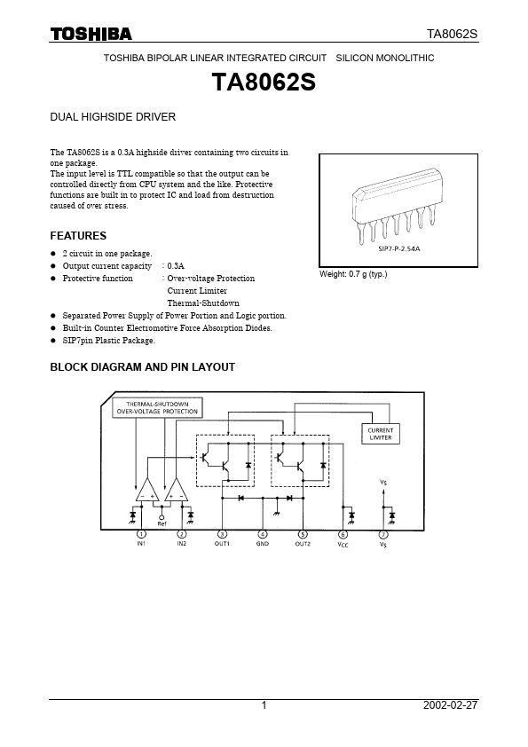
BLOCK DIAGRAM AND PIN LAYOUT
Weight: 0.7 g (typ.)
1 2002-02-27
TA8062S
PIN DESCRIPTION
PIN No.
1 2 3 5 4
6
7
SYMBOL
IN1 IN2 OUT1 OUT2 GND
VCC VS
DESCRIPTION
These terminals control output condition. The input level is TTL Compatible.
PNP-type complementary output pin with a current capacity of 0.3A. When the output pin is supplied with a current exceeding the detection current (typically 0.55A) because of load short-circuit, the output is limited to protect the IC.
Ground terminal
Power supply terminal for the output part of IC. Built-in over-
voltage function protects IC and load when the supplied
voltages higher than 30V.
Power supply terminal for the control part of IC and this pin is separated from VCC
MAXIMUM RATINGS (Ta = 25°C)
CHARACTERISTIC
Power Supply
Voltage Input
Voltage Output...