TB501-01/-05
www.DataSheet4U.com
Test Board for PLL501-01/-05
This note documents the test board prepared for the PLL50...
TB501-01/-05
www.DataSheet4U.com
Test Board for PLL501-01/-05
This note documents the test board prepared for the PLL501-01 and PLL501-05
The test board is designed to simplify the testing of the PLL501-01 and PLL501-05, and implements the best approaches for decoupling the VCXO chip using discrete external components. While this test board achieves satisfactory decoupling results, best results are achieved when the VCXO chip is laid out into the final PCB, following the recommendations indicated in the data sheet.
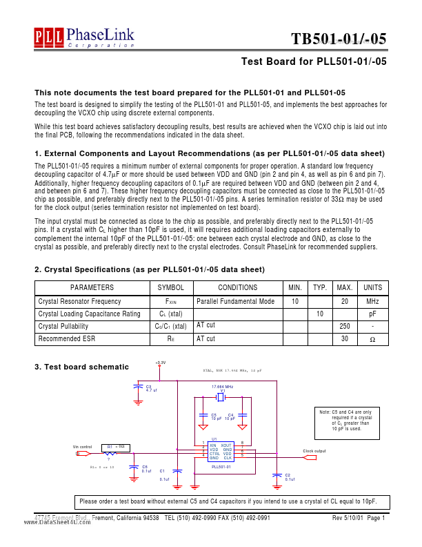
1. External Components and Layout Recommendations (as per PLL501-01/-05 data sheet)
The PLL501-01/-05 requires a minimum number of external components for proper operation. A standard low frequency decoupling capacitor of 4.7 µ F or more should be used between VDD and GND (pin 2 and pin 4, as well as pin 6 and pin 7). Additionally, higher frequency decoupling
capacitors of 0.1 µ F are required between VDD and GND (between pin 2 and 4, and between pin 6 and 7). These higher frequency decoupling
capacitors must be connected as close to the PLL501-01/-05 chip as possible, and preferably directly next to the PLL501-01/-05 pins. A series termination resistor of 33 Ω may be used for the clock output (series termination resistor not implemented on test board). The input crystal must be connected as close to the chip as possible, and preferably directly next to the PLL501-01/-05 pins. If a crystal with C L higher than 10pF is used, it will requires additional loading cap...