TC7MBL3125CFK,TC7MBL3126CFK
CMOS Digital Integrated Circuits Silicon Monolithic
TC7MBL3125CFK,TC7MBL3126CFK
1. Functiona...
TC7MBL3125CFK,TC7MBL3126CFK
CMOS Digital Integrated Circuits Silicon Monolithic
TC7MBL3125CFK,TC7MBL3126CFK
1. Functional Description
Low-
Voltage, Low-Capacitance Quad Bus Switch
2. General
The TC7MBL3125CFK and TC7MBL3126CFK are a low-
voltage/low-capacitance
CMOS 4bit Bus Switch. The low on-resistance of the switch allows connections to be made with minimal propagation delay time. The TC7MBL3125CFK requires the output enable (OE) input to be set high to place the output into the high impedance state, whereas the TC7MBL3126CFK requires the output enable (OE) input to be set low to place the output into the high impedance. All inputs are equipped with protection circuits against static discharge.
3. Features
(1) Operating
voltage: VCC = 1.65 to 3.6 V (2) ON capacitance: CI/O = 7.5 pF Switch On (typ.) @VCC = 3.0 V (3) ON resistance: RON = 6.5 Ω (typ.) @VCC = 3.0 V, VIS = 0 V (4) ESD performance: MM ≥ ±200 V, HBM ≥ ±2000 V (5) Power-down protection for inputs (OE, OE and I/O) (6) Package: VSSOP14 (US14)
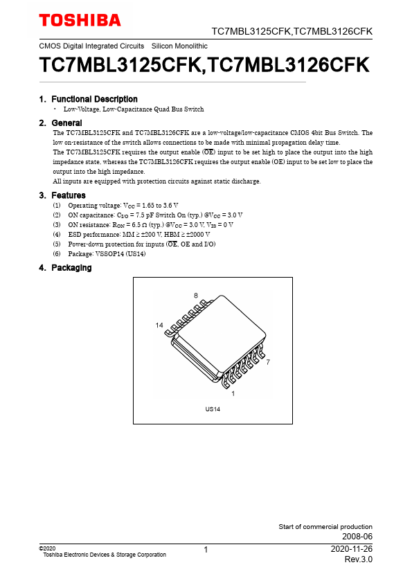
4. Packaging
US14
©2020
1
Toshiba Electronic Devices & Storage Corporation
Start of commercial production
2008-06
2020-11-26 Rev.3.0
5. Pin Assignment
TC7MBL3125CFK
TC7MBL3125CFK,TC7MBL3126CFK
TC7MBL3126CFK
6. Marking
TC7MBL3125CFK
7. System Diagram
TC7MBL3125CFK
TC7MBL3126CFK TC7MBL3126CFK
8. Truth Table
Inputs
Inputs
OE
OE
(TC7MBL3125CFK) (TC7MBL3126CFK)
L
H
H
L
Function
A port = B port Disconnect
©2020
2
Toshiba Electronic Devices & Storage Corporation...