TDA2824
DUAL POWER AMPLIFIER
. . . . .
SUPPLY VOLTAGE DOWN TO 3 V HIGH SVR LOW CROSSOVER DISTORTION LOW QUIESCENT CURR...
TDA2824
DUAL POWER AMPLIFIER
. . . . .
SUPPLY
VOLTAGE DOWN TO 3 V HIGH SVR LOW CROSSOVER DISTORTION LOW QUIESCENT CURRENT BRIDGE OR STEREO CONFIGURATION
Powerd ip (12+2+2)
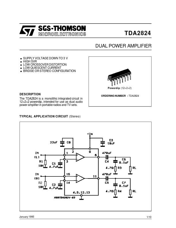
DESCRIPTION The TDA2824 is a monolithic integrated circuit in 12+2+2 powerdip, intended for use as dual audio power amplifier in portable radios and TV sets.
ORDERING NUMBER : TDA2824
TYPICAL APPLICATION CIRCUIT (Stereo)
R2
January 1995
1/10
TDA2824
PIN CONNECTION
SCHEMATIC DIAGRAM
ABSOLUTE MAXIMUM RATINGS
Symbol VS IO Ptot Tstg, Tj Supply
Voltage Output Peak Current Total Power Dissipation at Tamb = 50°C Tamb = 70°C Storage and Junction Temperature Parameter Value 16 1.5 1.25 4 -40 to 150 Unit V A W W °C
2/10
TDA2824
THERMAL DATA
Symbol R th j-amb Rth j-case Parameter Thermal Resistance Junction-ambient Thermal Resistance Junction-case Max. Max. Value 80 20 Un it °C/W °C/W
ELECTRICAL CHARACTERISTICS (VS = 6V, Tamb = 25°C, unless otherwise specified)
Symbol Parameter Test Co nditi ons Min. Typ . Max. Un it
STEREO (test circuit of fig. 1)
VS VO Id Ib PO Supply
Voltage Quiescent Output
Voltage Quiescent Drain Current Input Bias Current Output Power (each channel) d = 10% VS = 9V VS = 6V VS = 4.5V f = 1KHz RL = 4Ω RL = 4Ω RL = 4Ω 1.3 0.45 VS = 9V VS = 9V 3 4 2.7 6 100 1.7 0.65 0.32 0.2 36 100 B = 22Hz to 22KHz Curve A SVR CS Supply
Voltage Rejection Channel Separation f = 100Hz R S = 10KΩ f = 1KHz 40 2.5 2 50 50 39 41 12 15 V V V mA nA W W W % dB KΩ µV µV dB dB
d GV Ri eN
Distortion Closed Lo...