THC63LVDF84C_Rev.1.20_E
THC63LVDF84C
24bit Color LVDS Receiver (Falling Edge Strobe Output)
General Description
The THC...
THC63LVDF84C_Rev.1.20_E
THC63LVDF84C
24bit Color LVDS Receiver (Falling Edge Strobe Output)
General Description
The THC63LVDF84C receiver supports wide temperature range as -40 to +85C, and wide frequency range as 8 to 112MHz. The THC63LVDF84C converts the four LVDS data streams back into 24bits of LV
CMOS data with falling edge clock. At a transmit clock frequency of 112MHz, 24bits of RGB data and 4bits of timing and control data (HSYNC, VSYNC, DE, etc.) are transmitted at an effective rate of 3.1Gbps.
Application
・Medium and Small Size Panel ・Security Camera ・Multi Function Printer ・Machine Vision (Frame Grabber Board) ・Medical Equipment Monitor
Features
・1:7 LVDS to LV
CMOS Deserializer ・Operating Temperature Range : -40 to +85C ・No Special Start-up Sequence Required ・Spread Spectrum Clocking Tolerant up to 100kHz
Frequency Modulation and +/-2.5% Deviations ・Pixel Clock Range: 8 to 112MHz ・56pin TSSOP Package ・Power Down Mode ・Falling Edge Strobe Output ・EU RoHS Compliant
Recommended LVDS Transmitter ICs
・THC63LVDM83D ・THC63LVDM87
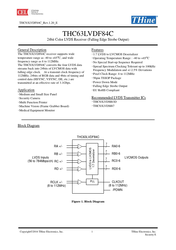
Block Diagram
RA +/RB +/LVDS Inputs (56 to 784Mbps/ch) RC +/RD +/-
THC63LVDF84C
LVDS to LV
CMOS 1:7 Deserializer
7
RA0-6
7
RB0-6 7 LV
CMOS Outputs
RC0-6
7
RD0-6
RCLK +/(8 to 112MHz)
PLL CLKOUT (8 to 112MHz)
/PDWN
Figure 1. Block Diagram
Copyright©2016 THine Electronics, Inc.
1
THine Electronics, Inc. Security E
THC63LVDF84C_Rev.1.20_E
Pin Diagram
RC3 RD6 RC4 GND RC5 RC6 RD0 LVDS GND RARA+ RBRB+ LVDS VCC LVDS GND RCRC+ RCLKRCLK+ RDRD+ ...