MOSFETs Silicon N-Channel MOS (π-MOS)
TK10X40D
1. Applications
• Switching Voltage Regulators
2. Features
(1) Low drain...
MOSFETs Silicon N-Channel MOS (π-MOS)
TK10X40D
1. Applications
Switching
Voltage Regulators
2. Features
(1) Low drain-source on-resistance: RDS(ON) = 0.46 Ω (typ.) (2) High forward transfer admittance: |Yfs| = 5.0 S (typ.) (3) Low leakage current: IDSS = 10 µA (max) (VDS = 400 V) (4) Enhancement mode: Vth = 2.0 to 4.0 V (VDS = 10 V, ID = 1 mA)
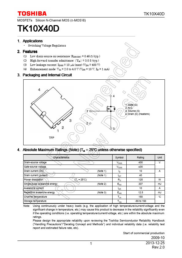
3. Packaging and Internal Circuit
TK10X40D
1: Gate (G) 2: N.C. 3: Source (S) 4: Drain (D) (Heatsink)
TFP
4. Absolute Maximum Ratings (Note) (Ta = 25 unless otherwise specified)
Characteristics
Symbol
Rating
Unit
Drain-source
voltage
VDSS
400
V
Gate-source
voltage
VGSS
±30
Drain current (DC)
(Note 1)
ID
10
A
Drain current (pulsed)
(Note 1)
IDP
40
Power dissipation
(Tc = 25)
PD
125
W
Single-pulse avalanche energy
(Note 2)
EAS
337
mJ
Avalanche current
IAR
10
A
Repetitive avalanche energy
(Note 3)
EAR
12.5
mJ
Channel temperature
Tch
150
Storage temperature
Tstg
-55 to 150
Note:
Using continuously under heavy loads (e.g. the application of high temperature/current/
voltage and the significant change in temperature, etc.) may cause this product to decrease in the reliability significantly even if the operating conditions (i.e. operating temperature/current/
voltage, etc.) are within the absolute maximum ratings. Please design the appropriate reliability upon reviewing the Toshiba Semiconductor Reliability Handbook ("Handling Precautions"/"Derating Concept and Methods") and individual re...