TK80D08K3 www.DataSheet4U.com
TOSHIBA Field Effect Transistor Silicon N Channel MOS Type (U-MOSⅣ)
TK80D08K3
Switching R...
TK80D08K3 www.DataSheet4U.com
TOSHIBA Field Effect Transistor Silicon N Channel MOS Type (U-MOSⅣ)
TK80D08K3
Switching Regulator Applications
Low drain-source ON-resistance: RDS (ON) = 3.6 mΩ (typ.) High forward transfer admittance: |Yfs| = 200 S Low leakage current: IDSS = 10 μA (max) (VDS = 75 V) Enhancement-mode: Vth = 2.0 to 4.0 V (VDS = 10 V, ID = 1 mA)
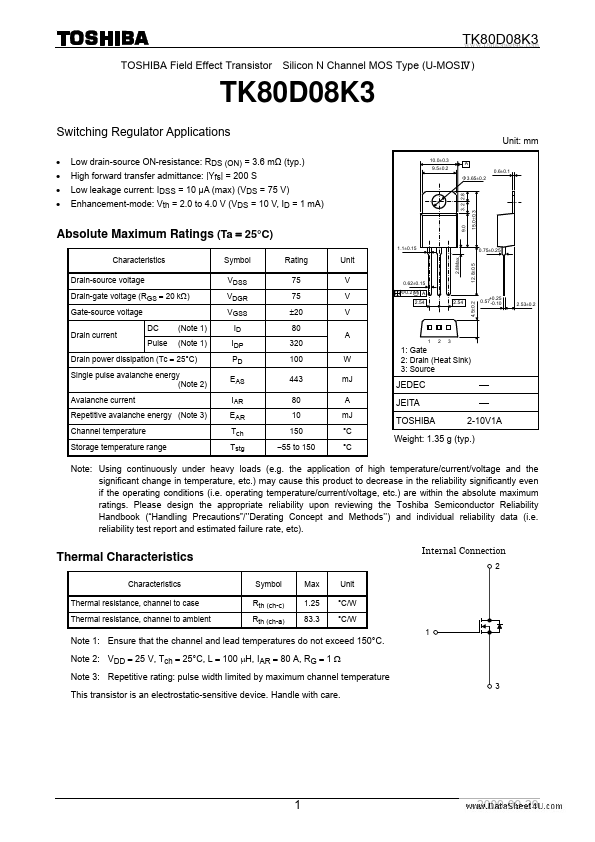
10.0±0.3 9.5±0.2 A 0.6±0.1 Ф3.65±0.2
Unit: mm
3.2 2.8 1.1±0.15 2.8Max. 9.0 15.0±0.3 0.75±0.25 12.8±0.5 +0.25 0.57 -0.10
Absolute Maximum Ratings (Ta = 25°C)
Characteristics Drain-source
voltage Drain-gate
voltage (RGS = 20 kΩ) Gate-source
voltage Drain current DC Pulse (Note 1) (Note 1) Symbol VDSS VDGR VGSS ID IDP PD EAS IAR EAR Tch Tstg Rating 75 75 ±20 80 320 100 443 80 10 150 −55 to 150 Unit V V V A W mJ A mJ °C °C
0.62±0.15 Ф0.2 M A
1
2
3
Drain power dissipation (Tc = 25°C) Single pulse avalanche energy (Note 2) Avalanche current Repetitive avalanche energy (Note 3) Channel temperature Storage temperature range
1: Gate 2: Drain (Heat Sink) 3: Source
4.5±0.2
2.54
2.54
2.53±0.2
JEDEC JEITA TOSHIBA
⎯ ⎯ 2-10V1A
Weight: 1.35 g (typ.)
Note: Using continuously under heavy loads (e.g. the application of high temperature/current/
voltage and the significant change in temperature, etc.) may cause this product to decrease in the reliability significantly even if the operating conditions (i.e. operating temperature/current/
voltage, etc.) are within the absolute maximum ratings. Please design the appropriat...