MOSFETs Silicon N-Channel MOS (π-MOS)
TK8P25DA
1. Applications
• Switching Voltage Regulators
2. Features
(1) Low drain...
MOSFETs Silicon N-Channel MOS (π-MOS)
TK8P25DA
1. Applications
Switching
Voltage Regulators
2. Features
(1) Low drain-source on-resistance: RDS(ON) = 0.41 Ω (typ.) (2) Low leakage current: IDSS = 10 µA (max) (VDS = 250 V) (3) Enhancement mode: Vth = 1.5 to 3.5 V (VDS = 10 V, ID = 1 mA)
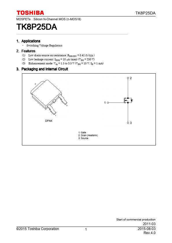
3. Packaging and Internal Circuit
TK8P25DA
DPAK
1: Gate 2: Drain (Heatsink) 3: Source
©2015 Toshiba Corporation
1
Start of commercial production
2011-03
2015-08-03 Rev.4.0
TK8P25DA
4. Absolute Maximum Ratings (Note) (Ta = 25 unless otherwise specified)
Characteristics
Symbol
Rating
Unit
Drain-source
voltage Gate-source
voltage Drain current (DC) Drain current (pulsed) Power dissipation Single-pulse avalanche energy Avalanche current Reverse drain current (DC) Reverse drain current (pulsed) Channel temperature Storage temperature
(Tc = 25)
(Note 1) (Note 1)
(Note 2) (Note 3) (Note 1) (Note 1)
VDSS VGSS
ID IDP PD EAS IAR IDR IDRP Tch Tstg
250
V
±20
7.5
A
30
55
W
45
mJ
7.5
A
7.5
30
150
-55 to 150
Note:
Using continuously under heavy loads (e.g. the application of high temperature/current/
voltage and the significant change in temperature, etc.) may cause this product to decrease in the reliability significantly even if the operating conditions (i.e. operating temperature/current/
voltage, etc.) are within the absolute maximum ratings. Please design the appropriate reliability upon reviewing the Toshiba Semiconductor Reliability Handbook ("Handling Precaution...