TLC5502Ć5M 8ĆBIT ANALOGĆTOĆDIGITAL CONVERTER
SGLS067 − MARCH 1992
• LinEPIC 1-µm CMOS Process • 8-Bit Resolution
J P...
TLC5502Ć5M 8ĆBIT ANALOGĆTOĆDIGITAL CONVERTER
SGLS067 − MARCH 1992
LinEPIC 1-µm
CMOS Process 8-Bit Resolution
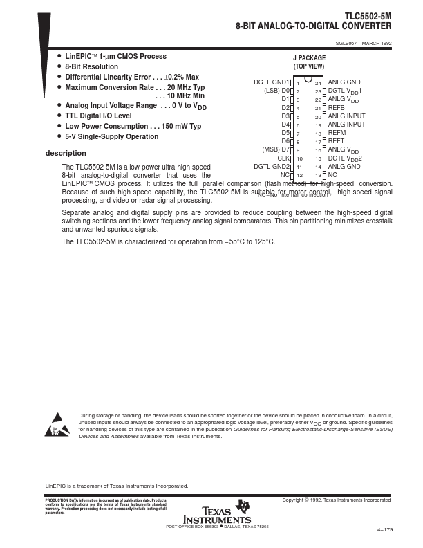
J PACKAGE (TOP VIEW)
Differential Linearity Error . . . ±0.2% Max Maximum Conversion Rate . . . 20 MHz Typ
. . . 10 MHz Min
Analog Input
Voltage Range . . . 0 V to VDD TTL Digital I/O Level
DGTL GND1 (LSB) D0 D1 D2 D3
1 2 3 4 5
24 ANLG GND
23 DGTL VDD1 22 ANLG VDD 21 REFB
20 ANLG INPUT
Low Power Consumption . . . 150 mW Typ 5-V Single-Supply Operation
D4 6 D5 7 D6 8
19 ANLG INPUT 18 REFM 17 REFT
description
(MSB) D7 9 CLK 10
16 ANLG VDD 15 DGTL VDD2
The TLC5502-5M is a low-power ultra-high-speed
DGTL GND2 11 14 ANLG GND
8-bit analog-to-digital converter that uses the
NC 12 13 NC
LinEPIC
CMOS process. It utilizes the full parallel comparison (flash method) for high-speed conversion.
Because of such high-speed capability, the TLC5502-5M is suNitCab−lNeofoinrtemrnaoltocroncnoencttioronl, high-speed signal processing, and video or radar signal processing.
Separate analog and digital supply pins are provided to reduce coupling between the high-speed digital switching sections and the lower-frequency analog signal comparators. This pin partitioning minimizes crosstalk and unwanted spurious signals.
The TLC5502-5M is characterized for operation from − 55°C to 125°C.
During storage or handling, the device leads should be shorted together or the device should be placed in conductive foam. In a circuit,
unused inputs should always be conne...