ą
TLV225xĆEP, TLV225xAĆEP
Advanced LinCMOS RAILĆTOĆRAIL
VERYĆLOWĆPOWER OPERATIONAL AMPLIFIERS
SGLS217B − NOVEMBER 2...
ą
TLV225xĆEP, TLV225xAĆEP
Advanced Lin
CMOS RAILĆTOĆRAIL
VERYĆLOWĆPOWER OPERATIONAL
AMPLIFIERS
SGLS217B − NOVEMBER 2003 − REVISED JUNE 2006
D Controlled Baseline
− One Assembly/Test Site, One Fabrication Site
D Extended Temperature Performance of
−40°C to 125°C
D Enhanced Diminishing Manufacturing
Sources (DMS) Support
D Enhanced Product-Change Notification D Qualification Pedigree† D ESD Protection Exceeds 2000 V Per
MIL-STD-883, Method 3015; Exceeds 150 V (TLV2252/52A) and 100 V (TLV2254/54A) Using Machine Model (C = 200 pF, R = 0)
† Component qualification in accordance with JEDEC and industry standards to ensure reliable operation over an extended temperature range. This includes, but is not limited to, Highly Accelerated Stress Test (HAST) or biased 85/85, temperature cycle, autoclave or unbiased HAST, electromigration, bond intermetallic life, and mold compound life. Such qualification testing should not be viewed as justifying use of this component beyond specified performance and environmental limits.
D Output Swing Includes Both Supply Rails D Low Noise . . . 19 nV/√Hz Typ at f = 1 kHz D Low Input Bias Current . . . 1 pA Typ D Fully Specified for Both Single-Supply and
Split-Supply Operation
D Very Low Power . . . 34 µA Per Channel
(Typ)
D Common-Mode Input
Voltage Range
Includes Negative Rail
D Low Input Offset
Voltage:
850 µV Max at TA = 25°C
D Wide Supply
Voltage Range:
2.7 V to 16 V
D Macromodel Included
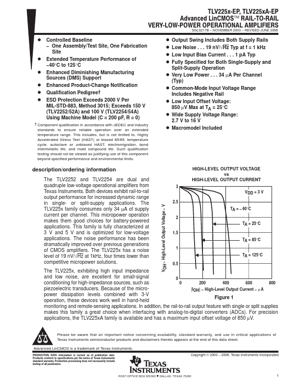
VOH − High-Level Output
Voltage − V
description/ord...