Product Folder
Sample & Buy
Technical Documents
Tools & Software
Support & Community
TLV341, TLV341A, TLV342, TLV34...
Product Folder
Sample & Buy
Technical Documents
Tools & Software
Support & Community
TLV341, TLV341A, TLV342, TLV342S
SLVS568D – JANUARY 2005 – REVISED APRIL 2016
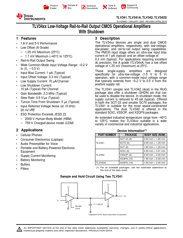
TLV34xx Low-
Voltage Rail-to-Rail Output
CMOS Operational
Amplifiers With Shutdown
1 Features
1 1.8-V and 5-V Performance Low Offset (A Grade)
– 1.25 mV Maximum (25°C) – 1.7 mV Maximum (–40°C to 125°C) Rail-to-Rail Output Swing Wide Common-Mode Input
Voltage Range: –0.2 V to (V+ – 0.5 V) Input Bias Current: 1 pA (Typical) Input Offset
Voltage: 0.3 mV (Typical) Low Supply Current: 70 μA/Channel Low Shutdown Current: 10 pA (Typical) Per Channel Gain Bandwidth: 2.3 MHz (Typical) Slew Rate: 0.9 V/μs (Typical) Turnon Time From Shutdown: 5 μs (Typical) Input Referred
Voltage Noise (at 10 kHz): 20 nV/√Hz ESD Protection Exceeds JESD 22 – 2000-V Human-Body Model (HBM) – 750-V Charged-device model (CDM)
2 Applications
Cellular Phones Consumer Electronics (Laptops) Audio Preamplifier for Voice Portable and Battery-Powered Electronic
Equipment Supply Current Monitoring Battery Monitoring Buffers Filters
3 Description
The TLV34xx devices are single and dual
CMOS operational
amplifiers, respectively, with low-
voltage, low-power, and rail-to-rail output swing capabilities. The PMOS input stage offers an ultra-low input bias current of 1 pA (typical) and an offset
voltage of 0.3 mV (typical). For applications requiring excellent dc precision, the A grade (TLV34xA) has a low offset volt...