Features Low gate charge 100% avalanche tested Improved dv/dt capability RoHS compliant Halogen free package ...
Features Low gate charge 100% avalanche tested Improved dv/dt capability RoHS compliant Halogen free package JEDEC Qualification
TMP8N50Z(G)/TMPF8N50Z(G)
BVDSS 500V
N-channel
MOSFET ID RDS(on) 8A <0.85W
Device TMP8N50Z/TMPF8N50Z TMP8N50ZG/TMPF8N50ZG
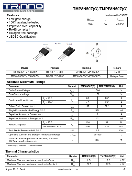
Package TO-220 / TO-220F TO-220 / TO-220F
Absolute Maximum Ratings
Parameter
Drain-Source
Voltage
Gate-Source
Voltage
Continuous Drain Current Pulsed Drain Current (Note 1)
TC = 25 ℃ TC = 100 ℃
Single Pulse Avalanche Energy (Note 2)
Repetitive Avalanche Current (Note 1)
Repetitive Avalanche Energy (Note 1)
Power Dissipation
TC = 25 ℃ Derate above 25 ℃
Peak Diode Recovery dv/dt (Note 3)
Operating Junction and Storage Temperature Range
Maximum lead temperature for soldering purposes, 1/8” from case for 5 seconds
* Limited only by maximum junction temperature
Marking TMP8N50Z/TMPF8N50Z TMP8N50ZG/TMPF8N50ZG
Remark RoHS
Halogen Free
Symbol VDSS VGS
ID
IDM EAS IAR EAR
PD
dv/dt TJ, TSTG
TL
TMP8N50Z(G) TMPF8N50Z(G) 500 ±30
8.0 8.0 * 4.5 4.5 * 32 32 *
554 8 12
120 39 0.96 0.31
4.5 -55~150
300
Unit V V A A A mJ A mJ W
W/℃ V/ns
℃
℃
Thermal Characteristics
Parameter Maximum Thermal resistance, Junction-to-Case Maximum Thermal resistance, Junction-to-Ambient
Symbol RqJC RqJA
August 2012 : Rev0
www.trinnotech.com
TMP8N50Z(G) 1.04 62.5
TMPF8N50Z(G) 3.2 62.5
Unit ℃/W ℃/W
1/7
TMP8N50Z(G)/TMPF8N50Z(G)
Electrical Characteristics : TC=25℃, unless otherwise noted
Parameter
Symbol
Test condition
Min T...