D Organization . . . 65 536 by 16 Bits D Single 5-V Power Supply D Operationally Compatible With Existing
Megabit EPROMs...
D Organization . . . 65 536 by 16 Bits D Single 5-V Power Supply D Operationally Compatible With Existing
Megabit EPROMs
D 40-Pin Dual-In-Line Package and 44-Lead
Plastic Leaded Chip Carrier
D All Inputs / Outputs Fully TTL Compatible D ±10% VCC Tolerance D Maximum Access / Minimum Cycle Time
’27C/PC210A-10 100 ns ’27C/ PC210A-12 120 ns ’27C/ PC210A-15 150 ns ’27C/ PC210A-20 200 ns ’27C/ PC210A-25 250 ns
D 16-Bit Output For Use in
Microprocessor-Based Systems
D Very High-Speed SNAP! Pulse
Programming
D Power-Saving
CMOS Technology D 3-State Output Buffers D 400-mV Minimum DC Noise Immunity With
Standard TTL Loads
D Latchup Immunity of 250 mA on All Input
and Output Pins
D No Pullup Resistors Required D Low Power Dissipation
− Active . . . 275 mW Worst Case − Standby . . . 0.55 mW Worst Case
(
CMOS-Input Levels)
D Temperature Range Options
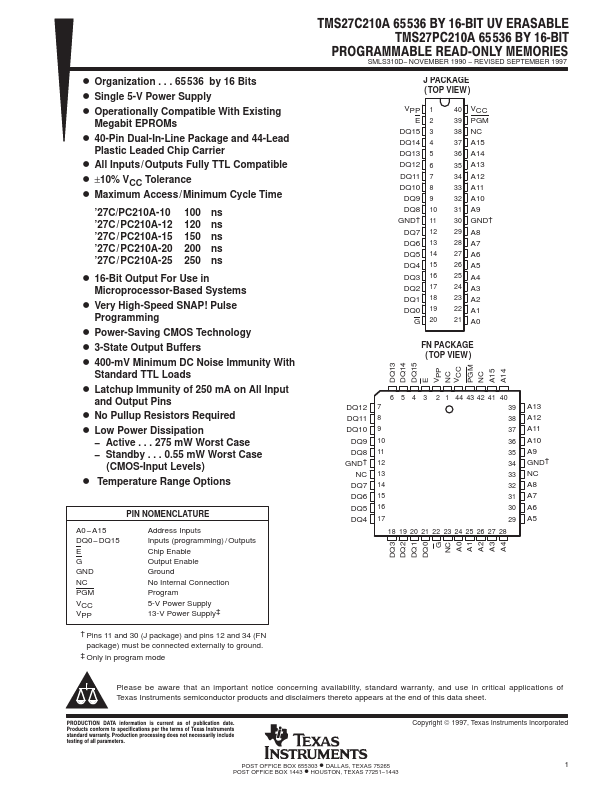
PIN NOMENCLATURE
A0 −A15 DQ0 −DQ15 E G GND NC PGM VCC VPP
Address Inputs Inputs (programming) / Outputs Chip Enable Output Enable Ground No Internal Connection Program 5-V Power Supply 13-V Power Supply‡
† Pins 11 and 30 (J package) and pins 12 and 34 (FN package) must be connected externally to ground.
‡ Only in program mode
DQ3 DQ2 DQ1 DQ0
G NC A0 A1 A2 A3 A4
TMS27C210A 65536 BY 16ĆBIT UV ERASABLE TMS27PC210A 65536 BY 16ĆBIT
PROGRAMMABLE READĆONLY MEMORIES SMLS310D− NOVEMBER 1990 − REVISED SEPTEMBER 1997
J PACKAGE ( TOP VIEW )
VPP E
DQ15 DQ14 DQ13 DQ12 DQ11 DQ10
DQ9 DQ8 GND† DQ7 DQ6 DQ5 DQ4 DQ3 DQ2 DQ1 DQ0
G
1 2 3 4 5 6 7 8 9 10 11...