FLASH MEMORIES
D Single Power Supply Supports 2.7-V and
3.6-V Read/Write Operation
D Organization . . . 1 048576 By 8 Bits D Array Bloc...
Description
D Single Power Supply Supports 2.7-V and
3.6-V Read/Write Operation
D Organization . . . 1 048576 By 8 Bits D Array Blocking Architecture
– One 16K-Byte Boot Sector
– Two 8K-Byte Parameter Sectors
– One 32K-Byte Sector
– Fifteen 64K-Byte Sectors
– Any Combination of Sectors Can Be
Erased. Supports Full-Chip Erase
– Any Combination of Sectors Can Be
Marked as Read-Only
D Boot-Code Sector Architecture
– T = Top Sector
– B = Bottom Sector
D Sector Protection
– Hardware Protection Method That
Disables Any Combination of Sectors
From Write or Erase Operations Using
Standard Programming Equipment
D Embedded Program/Erase Algorithms
– Automatically Pre-Programs and Erases
Any Sector
– Automatically Programs and Verifies the
Program Data at Specified Address
D JEDEC Standards
– Compatible With JEDEC Byte Pinouts
– Compatible With JEDEC EEPROM
Command Set
D Fully Automated On-Chip Erase and
Program Operations
D 100 000 Program/Erase Cycles D Low Power Dissipation D Low Current Consumption
– 20-mA Typical Active Read for Byte Mode
– 30-mA Typical Program / Erase Current – Less Than 60-µA Standby Current – 5 µA in Deep Power-Down Mode
TMS29LF008T, TMS29LF008B 1048576 BY 8-BIT FLASH MEMORIES
SMJS846A – MAY 1997 – REVISED NOVEMBER 1997
D All Inputs/Outputs TTL-Compatible D Erase Suspend/Resume
– Supports Reading Data From, or
Programming Data to, a Sector Not
Being Erased
D Hardware-Reset Pin Initializes the
Internal-State Machine to the Read
Operation
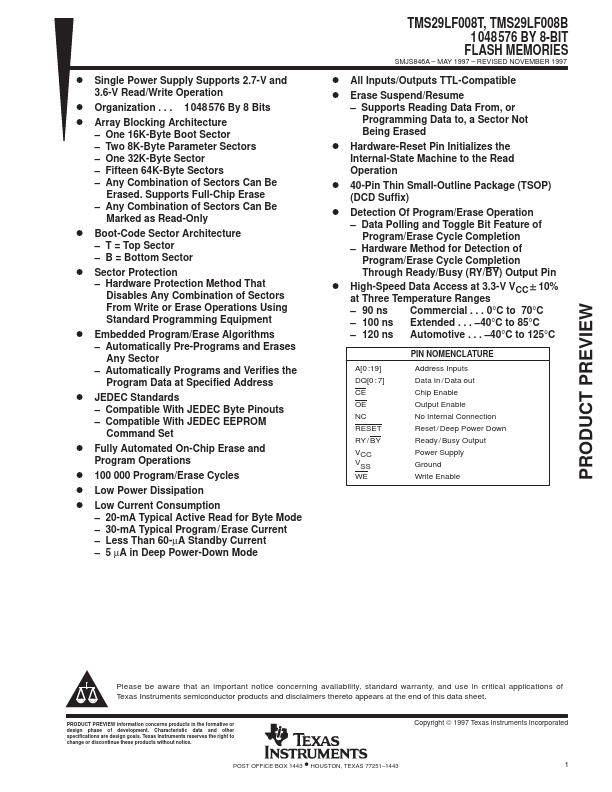
D 40-Pin Thin Small-Outline Package...
Similar Datasheet