This data sheet is applicable to all
TMS416100/Ps symbolized with Revision “B”
and subsequent revisions as described on
...
This data sheet is applicable to all
TMS416100/Ps symbolized with Revision “B”
and subsequent revisions as described on
page 24.
Organization . . . 16 777 216 × 1 Single 5-V Power Supply (±10% Tolerance) Performance Ranges:
’416100- 60 ’416100- 70
ACCESS ACCESS ACCESS READ
TIME TIME TIME OR WRITE
tRAC tCAC
tAA CYCLE
(MAX ) (MAX ) (MAX ) (MIN)
60 ns 15 ns 30 ns 110 ns
70 ns 18 ns 35 ns 130 ns
’416100- 80
80 ns 20 ns 40 ns 150 ns
Enhanced Page Mode Operation for Faster
Memory Access
CAS-Before-RAS Refresh
Long Refresh Period
– 4096 Cycle Refresh in 64 ms
(TMS416100)
– 256 ms for Extended Refresh Version
(TMS416100P)
3-State Unlatched Output
Low Power Dissipation (TMS416100P Only)
– 500-µA
CMOS Standby Current
– 500-µA Self-Refresh Current
– 500-µA Extended Refresh Battery Backup
Current
All Inputs, Outputs and Clocks Are TTL
Compatible
Operating Free-Air Temperature Range:
0°C to 70°C
TMS416100, TMS416100P 16 777 216-BIT
DYNAMIC RANDOM-ACCESS MEMORIES
SMKS611 – FEBRUARY 1994
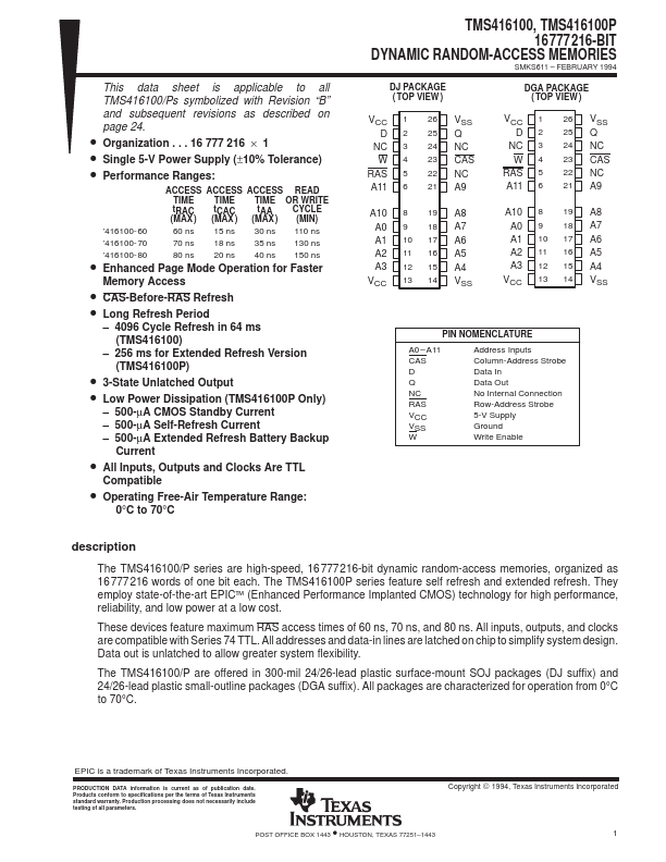
DJ PACKAGE ( TOP VIEW )
DGA PACKAGE ( TOP VIEW )
VCC D
NC W
RAS A11
1 2 3 4 5 6
26 VSS 25 Q 24 NC 23 CAS 22 NC 21 A9
VCC D
NC W
RAS A11
1 2 3 4 5 6
26 VSS 25 Q 24 NC 23 CAS 22 NC 21 A9
A10 8 19 A8 A0 9 18 A7 A1 10 17 A6 A2 11 16 A5 A3 12 15 A4
VCC 13 14 VSS
A10 8 19 A8 A0 9 18 A7 A1 10 17 A6 A2 11 16 A5 A3 12 15 A4
VCC 13 14 VSS
PIN NOMENCLATURE
A0 – A11
CAS
D
Q
NC
RAS
VCC VSS W
Address Inputs Column-Address Strobe Data In Data Out No Internal Co...