D Low rDS(on) . . . 0.3 Ω Typ D High Voltage Output . . . 60 V D Extended ESD Capability . . . 4000 V
TPIC5401 H-BRIDGE...
D Low rDS(on) . . . 0.3 Ω Typ D High
Voltage Output . . . 60 V D Extended ESD Capability . . . 4000 V
TPIC5401 H-BRIDGE GATE-PROTECTED
POWER DMOS ARRAY
SLIS024A – DECEMBER 1993 – REVISED MARCH 1994
D Pulsed Current . . . 10 A Per Channel D Fast Commutation Speed
description
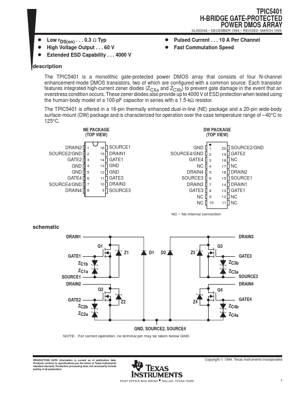
The TPIC5401 is a monolithic gate-protected power DMOS array that consists of four N-channel
enhancement-mode DMOS transistors, two of which are configured with a common source. Each transistor
features integrated high-current zener diodes (ZCXa and ZCXb) to prevent gate damage in the event that an overstress condition occurs. These zener diodes also provide up to 4000 V of ESD protection when tested using the human-body model of a 100-pF capacitor in series with a 1.5-kΩ resistor.
The TPIC5401 is offered in a 16-pin thermally enhanced dual-in-line (NE) package and a 20-pin wide-body
surface-mount (DW) package and is characterized for operation over the case temperature range of – 40°C to 125°C.
NE PACKAGE (TOP VIEW)
DW PACKAGE (TOP VIEW)
DRAIN2 SOURCE2/GND
GATE2 GND GND
GATE4 SOURCE4/GND
DRAIN4
1 2 3 4 5 6 7 8
16 SOURCE1 15 DRAIN1 14 GATE1 13 GND 12 GND 11 GATE3 10 DRAIN3 9 SOURCE3
GND SOURCE4/GND
GATE4 NC
DRAIN4 SOURCE3
DRAIN3 GATE3
NC NC
1 2 3 4 5 6 7 8 9 10
20 SOURCE2/GND 19 GATE2 18 NC 17 NC 16 DRAIN2 15 SOURCE1 14 DRAIN1 13 GATE1 12 NC 11 NC
NC – No internal connection
schematic
DRAIN1
GATE1 ZC1b ZC1a
SOURCE1 DRAIN2
GATE2 ZC2b ZC2a
Q1 Q2
Z1 Z2
D1 D2
DRAIN3
Q3 Z3
GATE3 ZC3b
ZC3a SOUR...