TPS1110, TPS1110Y SINGLE P-CHANNEL LOGIC-LEVEL MOSFETS
D Low rDS(on) . . . 65 mΩ Typ at VGS = – 4.5 V D High Current Ca...
TPS1110, TPS1110Y SINGLE P-CHANNEL LOGIC-LEVEL
MOSFETS
D Low rDS(on) . . . 65 mΩ Typ at VGS = – 4.5 V D High Current Capability
6 A at VGS = – 4.5 V
D Logic-Level Gate Drive (3 V Compatible)
VGS(th) = – 0.9 V Max
D Low Drain-Source Leakage Current
< 100 nA From 25°C to 75°C
at VDS = – 6 V
D Fast Switching . . . 5.8 ns Typ td(on) D Small-Outline Surface-Mount Power
Package
SLVS100B – OCTOBER 1994 – REVISED JANUARY 1998
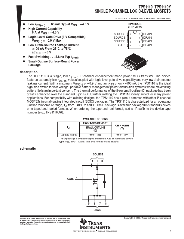
D PACKAGE (TOP VIEW)
SOURCE SOURCE SOURCE
GATE
1 2 3 4
8 DRAIN 7 DRAIN 6 DRAIN 5 DRAIN
description
The TPS1110 is a single, low-rDS(on), P-channel enhancement-mode power MOS transistor. The device features extremely low-rDS(on) values coupled with logic-level gate-drive capability and very low drain-source leakage current. With a maximum VGS(th) of – 0.9 V and an IDSS of only –100 nA, the TPS1110 is the ideal high-side switch for low-
voltage, portable battery-management power-distribution systems where maximizing
battery life is an important concern. The thermal performance of the 8-pin small-outline (D) package has been
greatly enhanced over the standard 8-pin SOIC, further making the TPS1110 ideally suited for many power
applications. For compatibility with existing designs, the TPS1110 has a pinout common with other P-channel
MOSFETs in small-outline integrated circuit (SOIC) packages. The TPS1110 is characterized for an operating junction temperature range, TJ, from – 40°C to 150°C. The D package is available packaged in standard sleeves or in taped an...