Product Folder
Sample & Buy
Technical Documents
Tools & Software
Support & Community
TPS22906
SLVS921A – MARCH 2009...
Product Folder
Sample & Buy
Technical Documents
Tools & Software
Support & Community
TPS22906
SLVS921A – MARCH 2009 – REVISED JULY 2015
TPS22906 Ultra-Small, Low-Input
Voltage, Low rON Load Switch
1 Features
2 Applications
1 Low-Input
Voltage: 1.0 V to 3.6 V
Ultra-Low ON-State Resistance
– rON = 90 mΩ at VIN = 3.6 V – rON = 100 mΩ at VIN = 2.5 V – rON = 114 mΩ at VIN = 1.8 V – rON = 172 mΩ at VIN = 1.2 V 500-mA Maximum Continuous Switch Current
Ultra-Low Quiescent Current: 82 nA at 1.8 V
Ultra-Low Shutdown Current: 44 nA at 1.8 V
Low Control Input Thresholds Enable Use of 1.2V/1.8-V/2.5-V/3.3-V Logic
Controlled Slew Rate to Avoid Inrush Current: 220 μs tr
ESD Performance Tested Per JESD 22
– 2000-V Human Body Model (A114-B, Class II)
– 1000-V Charged-Device Model (C101)
Four-Terminal Wafer-Chip-Scale Package (WCSP)
– 0.9 mm × 0.9 mm, 0.5-mm Pitch, 0.5-mm Height
Personal Digital Assistants (PDAs) Cellular Phones GPS Devices MP3 Players Digital Cameras Peripheral Ports Portable Instrumentation RF Modules
3 Description
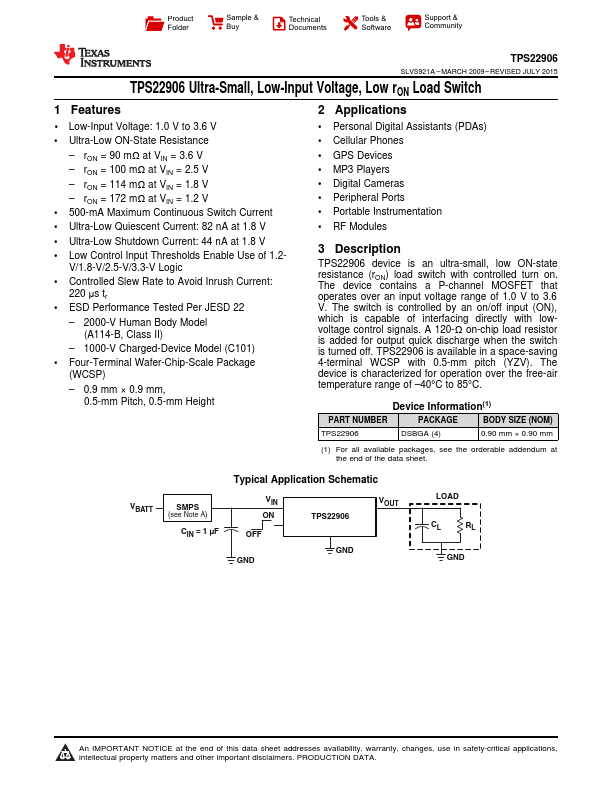
TPS22906 device is an ultra-small, low ON-state resistance (rON) load switch with controlled turn on. The device contains a P-channel
MOSFET that operates over an input
voltage range of 1.0 V to 3.6 V. The switch is controlled by an on/off input (ON), which is capable of interfacing directly with low
voltage control signals. A 120-Ω on-chip load resistor is added for output quick discharge when the switch is turned off. TP...