Product Folder
Sample & Buy
Technical Documents
Tools & Software
Support & Community
TPS22910A, TPS22912C, TPS22913...
Product Folder
Sample & Buy
Technical Documents
Tools & Software
Support & Community
TPS22910A, TPS22912C, TPS22913B, TPS22913C
SLVSB49F – NOVEMBER 2011 – REVISED JANUARY 2015
TPS2291xx Ultra-small, Low On Resistance Load Switch With Controlled Turn-on
1 Features
1 Integrated Single Load Switch Four Pin Wafer-Chip-Scale Package (Nom)
– 0.9 mm × 0.9 mm, 0.5-mm Pitch, 0.5-mm Height (YZV)
Input
Voltage Range: 1.4 V to 5.5 V Low ON-Resistance
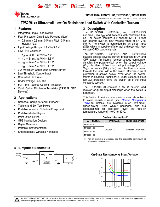
– rON = 60 mΩ at VIN = 5 V – rON = 61 mΩ at VIN = 3.3 V – rON = 74 mΩ at VIN = 1.8 V – rON = 84 mΩ at VIN = 1.5 V 2-A Maximum Continuous Switch Current Low Threshold Control Input Controlled Slew-rate Under-
Voltage Lock Out Full-Time Reverse Current Protection Quick Output Discharge Transistor (TPS22913B/C Devices)
2 Applications
Notebook Computer and Ultrabook™ Tablets and Set-Top-Boxes Portable Industrial / Medical Equipment Portable Media Players Point Of Sale Pins GPS Navigation Devices Digital Cameras Portable Instrumentation Smartphones / Wireless Handsets
3 Description
The TPS22910A, TPS22912C, and TPS22913B/C are small, low rON load switches with controlled turn on. The device contains a P-channel
MOSFET that can operate over an input
voltage range of 1.4 V to 5.5 V. The switch is controlled by an on/off input (ON), which is capable of interfacing directly with low
voltage GPIO control signals.
The TPS22910A, TPS22912C, and TPS22913B/C devices provide reverse current protection in ON and OFF...