Product Folder
Sample & Buy
Technical Documents
Tools & Software
Support & Community
TPS22932B
SLVS802C – AUGUST 20...
Product Folder
Sample & Buy
Technical Documents
Tools & Software
Support & Community
TPS22932B
SLVS802C – AUGUST 2009 – REVISED MAY 2015
TPS22932B Low Input
Voltage, Ultralow rON Load Switch With Configurable Enable Logic and Controlled Slew-Rate
1 Features
1 Input
Voltage: 1.1 V to 3.6 V Ultralow ON-Resistance
– rON = 55 mΩ at VIN = 3.6 V – rON = 65 mΩ at VIN = 2.5 V – rON = 75 mΩ at VIN = 1.8 V – rON = 115 mΩ at VIN = 1.2 V 500-mA Maximum Continuous Switch Current Quiescent Current < 1 μA Shutdown Current < 1 μA Low Control Threshold Allows Use of 1.2-V, 1.8-V, 2.5-V, and 3.3-V Logic Configurable Enable Logic Controlled Slew Rate to Avoid Inrush Currents: 165 μs at 1.8 V Six-Terminal Wafer Chip Scale Package (DSBGA) ESD Performance Tested Per JESD 22 – 2000-V Human-Body Model
(A114-B, Class II) – 1000-V Charged-Device Model (C101)
2 Applications
PDAs Cell Phones GPS Devices MP3 Players Digital Cameras Peripheral Ports Portable Instrumentation
3 Description
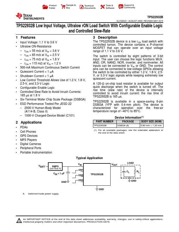
The TPS22932B device is a low rON load switch with controlled turnon. The device contains a P-channel
MOSFET that can operate over an input
voltage range of 1.1 V to 3.6 V.
The switch is controlled by eight patterns of 3-bit input. The user can choose the logic functions MUX, AND, OR, NAND, NOR, inverter, and noninverter. All inputs can be connected to VIN or GND. The control pins can be connected to low-
voltage GPIOs allowing the switch to be controlled by either 1.2-V, 1.8-V, 2.5V...