Product Folder
Sample & Buy
Technical Documents
Tools & Software
Support & Community
TPS22968-Q1
SLVSCP7B – NOVEMBE...
Product Folder
Sample & Buy
Technical Documents
Tools & Software
Support & Community
TPS22968-Q1
SLVSCP7B – NOVEMBER 2014 – REVISED MARCH 2016
TPS22968x-Q1 5.5-V, 4-A, 27-mΩ On-Resistance Load Switch
1 Features
1 Integrated Dual Channel Load Switch Qualified for Automotive Applications:
– Device Temperature Grade 1 : –40°C to +125°C Ambient Operating Temperature Range
Input
Voltage Range: 0.8 to 5.5 V VBIAS
Voltage Range: 2.5 to 5.5 V On-Resistance
– RON = 29 mΩ at VIN = 5 V (VBIAS = 5 V) – RON = 27 mΩ at VIN = 3.3 V (VBIAS = 5 V) – RON = 26 mΩ at VIN = 1.8 V (VBIAS = 5 V) 4-A Maximum Continuous Switch Current per Channel Low Quiescent Current
– 58-µA at VBIAS = 5 V (Both Channels) Low-Control Input-Threshold Enables Use of 1.2-,
1.8-, 2.5-, 3.3- V Logic Configurable Rise Time With CT Pin(1) Quick-Output Discharge (QOD)(2) (TPS22968-Q1
Only) 10-Pin WSON Package With Wettable Flanks ESD Performance Tested per JEDEC STD
– ±2-kV HBM and ±1-kV CDM Latch-Up Performance meets 100-mA per JESD
78, Class II GPIO Enable – Active High
(1) See Adjustable Rise Time for CT value versus rise time
(2) This feature discharges output of the switch to GND through a 270-Ω resistor, preventing the output from floating.
2 Applications
Automotive Electronics Infotainment Cluster ADAS
3 Description
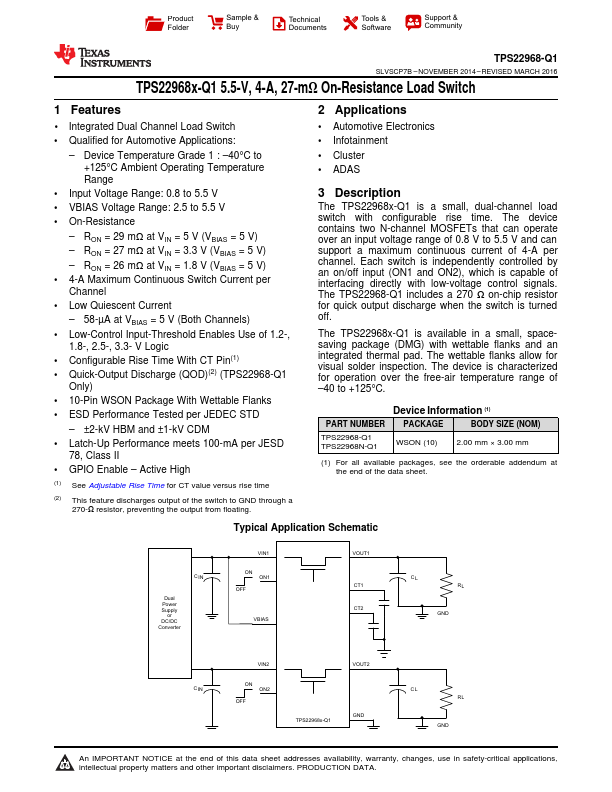
The TPS22968x-Q1 is a small, dual-channel load switch with configurable rise time. The device contains two N-channel
MOSFETs that can operate over an input volta...