Product Folder
Order Now
Technical Documents
Tools & Software
Support & Community
TPS22970
SLVSDF2A – MAY 2017 – RE...
Product Folder
Order Now
Technical Documents
Tools & Software
Support & Community
TPS22970
SLVSDF2A – MAY 2017 – REVISED JULY 2017
TPS22970 3.6-V, 4-A, 4.7-mΩ On-Resistance Load Switch
1 Features
1 Input
Voltage Range (VIN): 0.65 V to 3.6 V On-Resistance
– RON = 4.7 mΩ (Typical) at VIN ≥ 1.8 V – RON = 5.1 mΩ (Typical) at VIN = 1.05 V – RON = 6.4 mΩ (Typical) at VIN = 0.65 V Maximum Continuous Switch Current (IMAX): 4 A ON State (IQ): 30 µA (Typical) at VIN > 1.2 V OFF State (ISD): 1 µA (Typical) at VIN > 1.8 V Controlled Slew Rate to Avoid Inrush Current – 3.6 V Turn-ON time (tON): 1530 μs – 0.65 V Turn-ON time (tON): 815 μs Low Threshold Enable (ON) Supports Use of Logic as Low as 0.9 V (VIH) of Logic Thermal Shutdown (TSD) Quick Output Discharge (QOD): 150-Ω (Typical)
2 Applications
Notebook, Tablet Industrial PC Smartphones Telecom Storage
3 Description
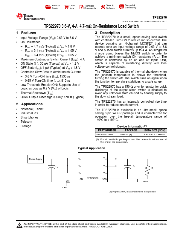
The TPS22970 is a small, space-saving load switch with controlled Turn-ON to reduce inrush current. The device contains an N-channel
MOSFET that can operate over an input
voltage range of 0.65 V to 3.6 V and pulsed switch currents up to 4 A. An integrated charge pump biases the NMOS switch in order to achieve a minimum switch ON resistance (RON). The switch is controlled by an on and off input (ON), which is capable of interfacing directly with low
voltage control signals.
The TPS22970 is capable of thermal shutdown when the junction temperature is above the threshold, turning the switch off...