Product Folder
Sample & Buy
Technical Documents
Tools & Software
Support & Community
TPS61253, TPS61254, TPS61256, ...
Product Folder
Sample & Buy
Technical Documents
Tools & Software
Support & Community
TPS61253, TPS61254, TPS61256, TPS61258, TPS61259, TPS612592
SLVSAG8G – SEPTEMBER 2011 – REVISED JUNE 2016
TPS6125x 3.5-MHz High Efficiency Step-Up Converter In Chip Scale Packaging
1 Features
1 93% Efficiency at 3.5-MHz Operation 21-µA Quiescent Current in Standby Mode 37-µA Quiescent Current in Normal Operation Wide VIN Range From 2.3 V to 5.5 V VIN ≥ VOUT Operation IOUT ≥ 800 mA at VOUT = 4.5 V, VIN ≥ 2.65 V IOUT ≥ 1000 mA at VOUT = 5.0 V, VIN ≥ 3.3 V IOUT ≥ 1500 mA (Peak) at VOUT = 5.0 V, VIN ≥ 3.3
V ±2% Total DC
Voltage Accuracy Light-Load PFM Mode Selectable Standby Mode or True Load
Disconnect During Shutdown Thermal Shutdown and Overload Protection Only Three Surface-Mount External Components
Required Total Solution Size < 25 mm2 9-Pin NanoFreeTM (CSP) Packaging
2 Applications
Cell Phones, Smart Phones Mono and Stereo APA Applications USB Charging Ports (5V)
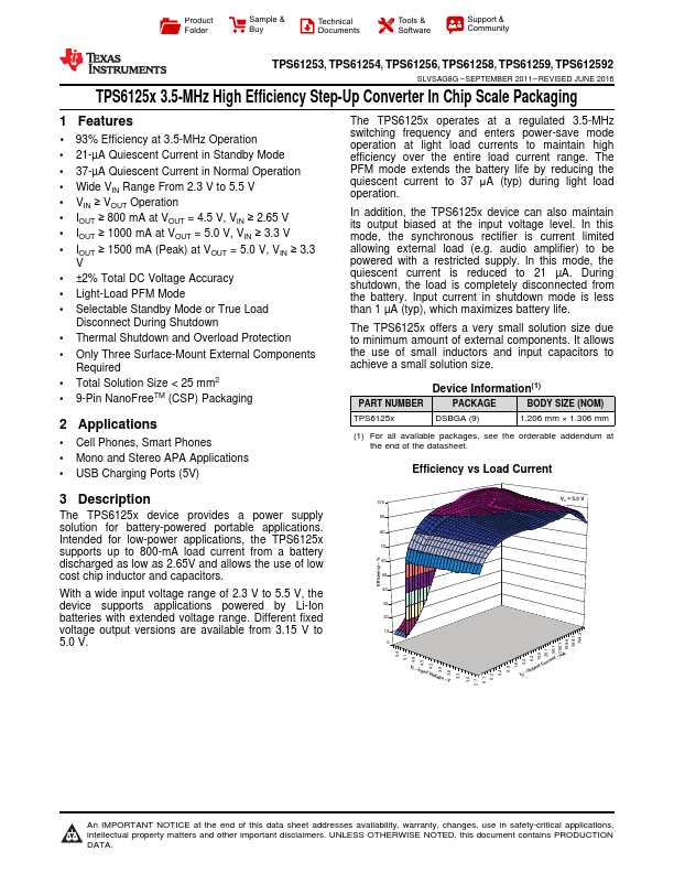
The TPS6125x operates at a regulated 3.5-MHz switching frequency and enters power-save mode operation at light load currents to maintain high efficiency over the entire load current range. The PFM mode extends the battery life by reducing the quiescent current to 37 μA (typ) during light load operation.
In addition, the TPS6125x device can also maintain its output biased at the input
voltage level. In this mode, the synchronous rectifier is current limited allowing external load (e.g. audio...