TPS9103 POWER SUPPLY FOR GaAs POWER AMPLIFIERS
D Charge Pump Provides Negative Gate Bias
for Depletion-Mode GaAs Power ...
TPS9103 POWER SUPPLY FOR GaAs POWER
AMPLIFIERS
D Charge Pump Provides Negative Gate Bias
for Depletion-Mode GaAs Power
Amplifiers
D Buffered Clock Output to Drive Additional
External Charge Pump
D 135-mΩ High-Side Switch Controls Supply
Voltage to the GaAs Power Amplifier
D Power-Good Circuitry Prevents High-Side
Switch Turn-on Until Negative Gate Bias is
Present
D Charge Pump Can Be Driven From the
Internal Oscillator or An External Clock
D 10-µA Maximum Standby Current D Low-Profile (1.2-mm Max Height), 20-Pin
TSSOP Package
GATE_BIAS VCC C1– C1+
BATT_IN BATT_IN BATT_IN
PGP PG
GND
SLVS131A – OCTOBER 1995 – REVISED JULY 1996
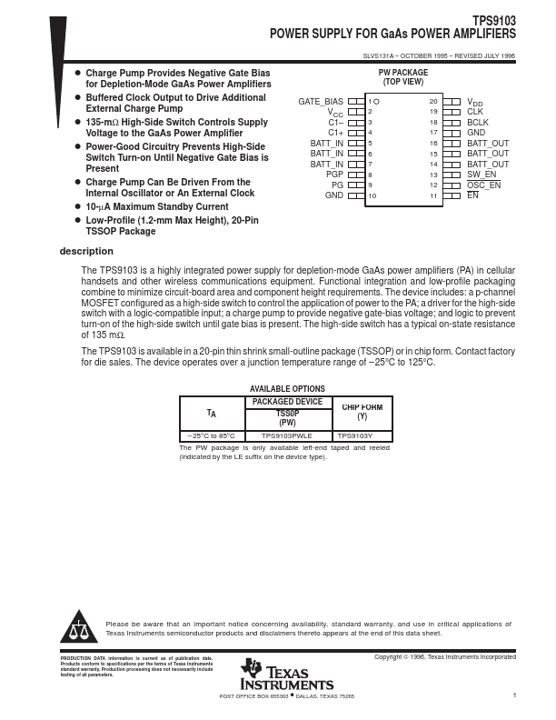
PW PACKAGE (TOP VIEW)
1 20 VDD 2 19 CLK 3 18 BCLK 4 17 GND 5 16 BATT_OUT 6 15 BATT_OUT 7 14 BATT_OUT 8 13 SW_EN 9 12 OSC_EN 10 11 EN
description
The TPS9103 is a highly integrated power supply for depletion-mode GaAs power
amplifiers (PA) in cellular handsets and other wireless communications equipment. Functional integration and low-profile packaging combine to minimize circuit-board area and component height requirements. The device includes: a p-channel
MOSFET configured as a high-side switch to control the application of power to the PA; a driver for the high-side switch with a logic-compatible input; a charge pump to provide negative gate-bias
voltage; and logic to prevent turn-on of the high-side switch until gate bias is present. The high-side switch has a typical on-state resistance of 135 mΩ.
The TPS9103 is available in a 20-pin thin shrink s...