11-Output Configurable Clock Buffer
T
R
I
Q
U
I
N
T
S E M I C O N D U C T O R, I N C .
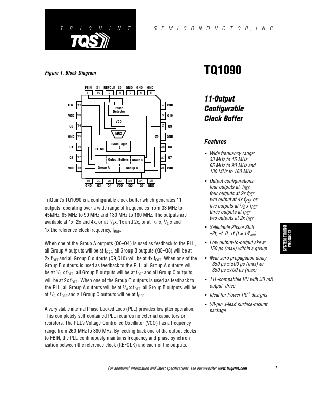
Figure 1. Block Diagram
FBIN
11
TQ1090
S1
10
REFCLK S0
9 8...
Description
T
R
I
Q
U
I
N
T
S E M I C O N D U C T O R, I N C .
Figure 1. Block Diagram
FBIN
11
TQ1090
S1
10
REFCLK S0
9 8
GND
7
GND
6
GND
5
TEST 12 VDD 13
Phase Detector VCO
4 VDD 3 2
Q10 Q9
11-Output Configurable Clock Buffer
Features
Q0
14
GND 15 Q1 Q2
16 17
MUX Divide Logic ÷2 Output Buffers Group C Group A Group B
1 GND 28 27
S1 S0
Q8 Q7
VDD 18
26 VDD
Wide frequency range: 33 MHz to 45 MHz 65 MHz to 90 MHz and 130 MHz to 180 MHz Output configurations: four outputs at fREF four outputs at 2x fREF two output at 4x fREF or five outputs at 1/2 x fREF three outputs at fREF two outputs at 2x fREF Selectable Phase Shift: –2t, –t, 0, +t (t = 1/fvco) Low output-to-output skew: 150 ps (max) within a group Near-zero propagation delay –350 ps ± 500 ps (max) or –350 ps ±700 ps (max) TTL-compatible I/O with 30 mA output drive Ideal for Power PC™ designs 28-pin J-lead surface-mount package
SYSTEM TIMING PRODUCTS
19
20
21
22
23
24
25
GND
Q3
Q4
VDD
Q5
Q6
GND
TriQuint’s TQ1090 is a configurable clock buffer which generates 11 outputs, operating over a wide range of frequencies from 33 MHz to 45MHz, 65 MHz to 90 MHz and 130 MHz to 180 MHz. The outputs are available at 1x, 2x and 4x, or at 1/2x, 1x and 2x, or at 1/4 x, 1/2 x and 1x the reference clock frequency, fREF. When one of the Group A outputs (Q0–Q4) is used as feedback to the PLL, all Group A outputs will be at fREF, all Group B outputs (Q5–Q8) will be at 2x fREF and all Group C outputs...
Similar Datasheet