®
TS272C,I,M
HIGH SPEED CMOS DUAL OPERATIONAL AMPLIFIERS
. . . . .
OUTPUT VOLTAGE CAN SWING GROUND EXCELLENT PHASE MA...
®
TS272C,I,M
HIGH SPEED
CMOS DUAL OPERATIONAL
AMPLIFIERS
. . . . .
OUTPUT
VOLTAGE CAN SWING GROUND EXCELLENT PHASE MARGIN ON CAPACITIVE LOADS GAIN BANDWIDTH PRODUCT / 3.5MHz STABLE AND LOW OFFSET
VOLTAGE THREE INPUT OFFSET
VOLTAGE SELECTIONS
TO
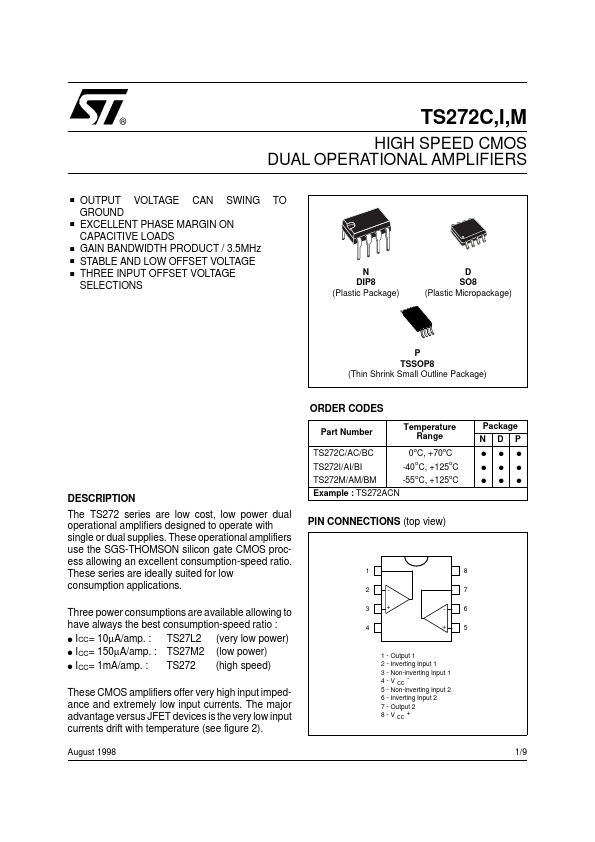
N DIP8 (Plastic Package)
D SO8 (Plastic Micropackage)
P TSSOP8 (Thin Shrink Small Outline Package)
ORDER CODES
Part Number TS272C/AC/BC TS272I/AI/BI TS272M/AM/BM Example : TS272ACN Temperature Range 0 C, +70 C -40oC, +125oC -55oC, +125oC
o o
Package N
q q q
D
q q q
P
q q q
DESCRIPTION The TS272 series are low cost, low power dual operational
amplifiers designed to operate with single or dual supplies. These operational
amplifiers use the SGS-THOMSON silicon gate
CMOS process allowing an excellent consumption-speed ratio. These series are ideally suited for low consumption applications. Three power consumptions are available allowing to have always the best consumption-speed ratio : q ICC= 10µA/amp. : TS27L2 (very low power) q ICC= 150µA/amp. : TS27M2 (low power) q ICC= 1mA/amp. : TS272 (high speed) These
CMOS amplifiers offer very high input impedance and extremely low input currents. The major advantage versus JFET devices is the very low input currents drift with temperature (see figure 2).
August 1998
PIN CONNECTIONS (top view)
1 2 3 4 + +
8 7 6 5
1 - Output 1 2 - Inverting Input 1 3 - Non-inverting Input 1 4-V
CC
5 - Non-inverting Input 2 6 - Inverting Input 2 7 - Output 2 8 - V CC +
1/9
TS272C,I,M
BLOCK DIAGRAM
...