TS522
PRECISION LOW NOISE DUAL OPERATIONAL AMPLIFIERS
. . . . . .
LOW INPUT OFFSET VOLTAGE 850µV max. LOW VOLTAGE NOIS...
TS522
PRECISION LOW NOISE DUAL OPERATIONAL
AMPLIFIERS
. . . . . .
LOW INPUT OFFSET
VOLTAGE 850µV max. LOW
VOLTAGE NOISE : 4.5nV/ √ Hz HIGH GAIN BANDWIDTH PRODUCT : 15MHz HIGH SLEW RATE : 7V/µs LOW DISTORTION : 0.002% ESD INTERNAL PROTECTION 2kV
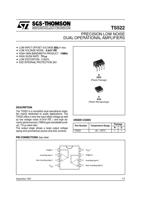
N DIP8 (Plastic Package)
D SO8 (Plastic Micropackage)
DESCRIPTION The TS522 is a monolithic dual operational amplifier mainly dedicated to audio applications. The TS522 offers a very low input offset
voltage as well as low
voltage noise (4.5nV/√ Hz ) and high dynamic performances (15MHz gain bandwidth product, 7V/µs slew rate). The output stage allows a large output
voltage swing and symmetrical source and sink currents. PIN CONNECTIONS (top view)
ORDER CODES
Part Number TS522I Temperature Range -40, +125oC Package N D
Output 1
Inverting input 1 Non-inverting input 1
1 2 3
+ +
8 7 6 5
VCC+
Output 2 Inverting input 2 Non-inverting input 2
- 4 V CC
September 1997
1/5
TS522
SCHEMATIC DIAGRAM (1/2 TS522)
VCC
Output Inverting Input Non-inverting Input
VCC
ABSOLUTE MAXIMUM RATINGS
Symbol VCC Vid Vi Toper Tj Tstg Ptot
Notes :
Parameter Supply
Voltage Differential Input
Voltage - (note 1) Input
Voltage - (note 1) Output Short-Circuit Duration - (note 2) Operating Free-air Temperature Range Maximum Junction Temperature Storage Temperature Maximum Power Dissipation - (note 2)
Value ±18 or +36 ±30 ±15 Infinite -40 to +105 +150 -65 to +150 500
Unit V V V
o o o
C C C
mW
1. Either or both input
voltages must ...