TSP2N60M / TSF2N60M
600V N-Channel MOSFET
General Description
This Power MOSFET is produced using Truesemi‘s advanced p...
TSP2N60M / TSF2N60M
600V N-Channel
MOSFET
General Description
This Power
MOSFET is produced using Truesemi‘s advanced planar stripe DMOS technology. This advanced technology has been especially tailored to minimize on-state resistance, provide superior switching performance, and withstand high energy pulse in the avalanche and commutation mode. These devices are well suited for high efficiency switched mode power supplies, active power factor correction based on half bridge topology.
Features
2.0A, 600V, RDS(on) = 5.00 @VGS = 10 V Low gate charge ( typical 9nC) High ruggedness Fast switching 100% avalanche tested Improved dv/dt capability
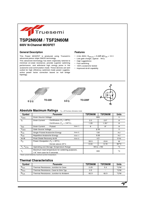
D
GDS
TO-220
GD S
TO-220F
●
◀▲ G ●
●
S
Absolute Maximum Ratings TC = 25°Cunless otherwise noted
Symbol
Parameter
VDSS
Drain-Source
Voltage
ID Drain Current - Continuous (TC = 25°C)
- Continuous (TC = 100°C)
IDM Drain Current - Pulsed
(Note 1)
VGSS
Gate-Source
Voltage
EAS Single Pulsed Avalanche Energy
(Note 2)
EAR Repetitive Avalanche Energy
(Note 1)
dv/dt
Peak Diode Recovery dv/dt
(Note 3)
PD Power Dissipation (TC = 25°C)
- Derate above 25°C
TJ, TSTG
Operating and Storage Temperature Range
TL
Maximum lead temperature for soldering purposes, 1/8" from case for 5 seconds
* Drain current limited by maximum junction temperature.
TSP2N60M TSF2N60M 600
2.0 2.0* 1.35 1.35 *
8 8* 30 130 5.55 4.5
55.5 23.6 0.44 0.19
-55 to +150
300
Thermal Characteristics
Symbol RJC RCS RJA
Parameter Thermal ...