Product Folder
Order Now
Technical Documents
Tools & Software
Support & Community
UCC21225A
SLUSCV6A – APRIL 2017 –...
Product Folder
Order Now
Technical Documents
Tools & Software
Support & Community
UCC21225A
SLUSCV6A – APRIL 2017 – REVISED FEBRUARY 2018
UCC21225A 4-A, 6-A, 2.5-kVRMS Isolated Dual-Channel Gate Driver in LGA
1 Features
1 Universal: Dual Low-Side, Dual High-Side or HalfBridge Driver
5 x 5 mm, Space-Saving LGA-13 Package Switching Parameters:
– 19-ns Typical Propagation Delay – 5-ns Maximum Delay Matching – 6-ns Maximum Pulse-Width Distortion CMTI Greater than 100-V/ns 4-A Peak Source, 6-A Peak Sink Output TTL and
CMOS Compatible Inputs 3-V to 18-V Input VCCI Range Up to 25-V VDD with 5-V UVLO Programmable Overlap and Dead Time Rejects Input Transients Shorter than 5-ns Fast Disable for Power Sequencing Safety-Related Certifications: – 3535-VPK Isolation per DIN V VDE V 0884-
11:2017-01 – 2500-VRMS Isolation for 1 Minute per UL 1577 – CQC per GB4943.1-2011 (Planned)
3 Description
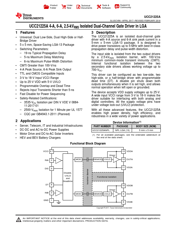
The UCC21225A is an isolated dual-channel gate driver with 4-A source and 6-A sink peak current in a 5-mm x 5-mm LGA-13 package. It is designed to drive power transistors up to 5-MHz with best-in-class propagation delay and pulse-width distortion.
The input side is isolated from the two output drivers by a 2.5-kVRMS isolation barrier, with 100-V/ns minimum common-mode transient immunity (CMTI). Internal functional isolation between the two secondary side drivers allows working
voltage up to 700-VDC.
This driver can be configured as two low-side, two high-side, or a half-...