Product Folder
Sample & Buy
Technical Documents
Tools & Software
Support & Community
UCC27517A-Q1
SLVSC88B – AUGUST...
Product Folder
Sample & Buy
Technical Documents
Tools & Software
Support & Community
UCC27517A-Q1
SLVSC88B – AUGUST 2013 – REVISED AUGUST 2015
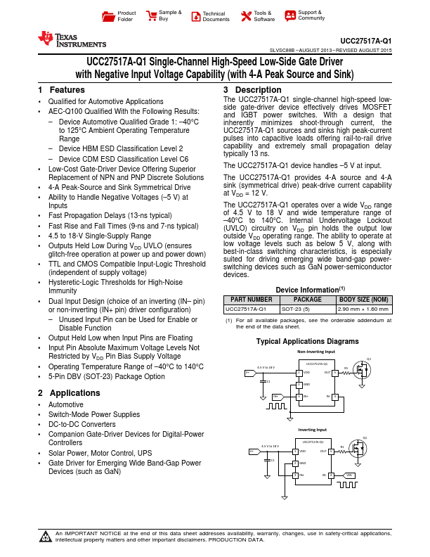
UCC27517A-Q1 Single-Channel High-Speed Low-Side Gate Driver with Negative Input
Voltage Capability (with 4-A Peak Source and Sink)
1 Features
1 Qualified for Automotive Applications AEC-Q100 Qualified With the Following Results:
– Device Automotive Qualified Grade 1: –40°C to 125°C Ambient Operating Temperature Range
– Device HBM ESD Classification Level 2 – Device CDM ESD Classification Level C6 Low-Cost Gate-Driver Device Offering Superior Replacement of NPN and PNP Discrete Solutions 4-A Peak-Source and Sink Symmetrical Drive Ability to Handle Negative
Voltages (–5 V) at Inputs Fast Propagation Delays (13-ns typical) Fast Rise and Fall Times (9-ns and 7-ns typical) 4.5 to 18-V Single-Supply Range Outputs Held Low During VDD UVLO (ensures glitch-free operation at power up and power down) TTL and
CMOS Compatible Input-Logic Threshold (independent of supply
voltage) Hysteretic-Logic Thresholds for High-Noise Immunity Dual Input Design (choice of an inverting (IN– pin) or non-inverting (IN+ pin) driver configuration) – Unused Input Pin can be Used for Enable or
Disable Function Output Held Low when Input Pins are Floating Input Pin Absolute Maximum
Voltage Levels Not
Restricted by VDD Pin Bias Supply
Voltage Operating Temperature Range of –40°C to 140°C 5-Pin DBV (SOT-23) Package Option
2 Application...