V20150SG-E3, VF20150SG-E3, VB20150SG-E3, VI20150SG-E3
www.vishay.com
Vishay General Semiconductor
High Voltage Trench...
V20150SG-E3, VF20150SG-E3, VB20150SG-E3, VI20150SG-E3
www.vishay.com
Vishay General Semiconductor
High
Voltage Trench MOS Barrier Schottky Rectifier
Ultra Low VF = 0.57 V at IF = 5 A
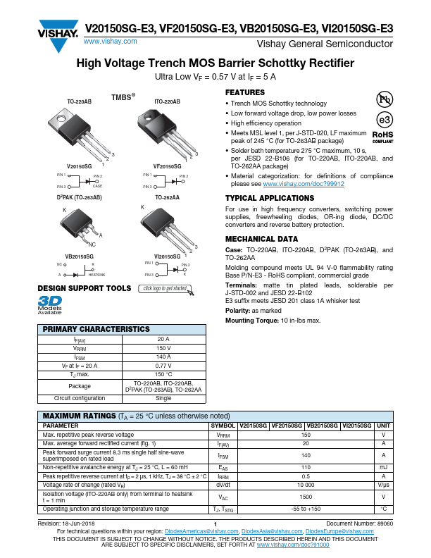
TO-220AB
TMBS ®
ITO-220AB
V20150SG
3 2 1
PIN 1
PIN 2
PIN 3
CASE
D2PAK (TO-263AB)
K
123 VF20150SG
PIN 1
PIN 2
PIN 3
TO-262AA K
A NC VB20150SG
NC K A HEATSINK
DESIGN SUPPORT TOOLS
3 2 VI20150SG 1
PIN 1
PIN 2
PIN 3
K
click logo to get started
Models
Available
PRIMARY CHARACTERISTICS
IF(AV) VRRM IFSM VF at IF = 20 A TJ max.
Package
20 A 150 V 140 A 0.77 V 150 °C TO-220AB, ITO-220AB, D2PAK (TO-263AB), TO-262AA
Circuit configuration
Single
FEATURES
Trench MOS Schottky technology Low forward
voltage drop, low power losses High efficiency operation Meets MSL level 1, per J-STD-020, LF maximum
peak of 245 °C (for TO-263AB package) Solder bath temperature 275 °C maximum, 10 s,
per JESD 22-B106 (for TO-220AB, ITO-220AB, and TO-262AA package) Material categorization: for definitions of compliance please see www.vishay.com/doc?99912
TYPICAL APPLICATIONS
For use in high frequency converters, switching power supplies, freewheeling diodes, OR-ing diode, DC/DC converters and reverse battery protection.
MECHANICAL DATA Case: TO-220AB, ITO-220AB, D2PAK (TO-263AB), and TO-262AA Molding compound meets UL 94 V-0 flammability rating Base P/N-E3 - RoHS compliant, commercial grade Terminals: matte tin plated leads, solderable per J-STD-002 and JESD 22-B102 E3 suffix meets JES...